Method for fabricating photo sensor

a technology of photosensors and manufacturing methods, applied in the direction of basic electric elements, electrical equipment, semiconductor devices, etc., can solve the problems of limiting the application and productivity of traditional pin photodiodes, poor signal-to-noise ratio, and low light receiving efficiency, so as to reduce the manufacturing cost of amorphous silicon tft display panels and improve product reliability

Active Publication Date: 2010-09-07
OPTRONIC SCI LLC
View PDF14 Cites 44 Cited by
  • Summary
  • Abstract
  • Description
  • Claims
  • Application Information

AI Technical Summary

Benefits of technology

[0006]It is therefore one of the objectives of the present invention to provide a method of fabricating a photo sensor integrated into the process of an amorphous silicon TFT. The photo sensor of the present invention uses silicon-rich dielectric material, and thus the product reliability is substantially improved.
[0008]The photo sensor of the present invention uses silicon-rich dielectric material, and the method of the present invention is integrated into the fabrication of amorphous silicon TFT. Consequently, the overall manufacturing cost of amorphous silicon TFT display panel is reduced, and the product reliability is improved.

Problems solved by technology

The PIN photodiode, however, has low light receiving efficiency and tends to be influenced by untargeted light sources, and thus suffers disadvantages, e.g. poor signal-to-noise ratio.
In addition, the IIIA material and VA material of the PIN photodiode and the TFT fabrication have compatibility problems, which limit the application and productivity of the traditional PIN photodiode.
The amorphous silicon TFT sensor, however, has low photo-current stability, which means the photo current decays with time even when the sensor is not operated.
Therefore, the reliability is low.

Method used


Image

  • Method for fabricating photo sensor
  • Method for fabricating photo sensor
  • Method for fabricating photo sensor

Examples


first embodiment

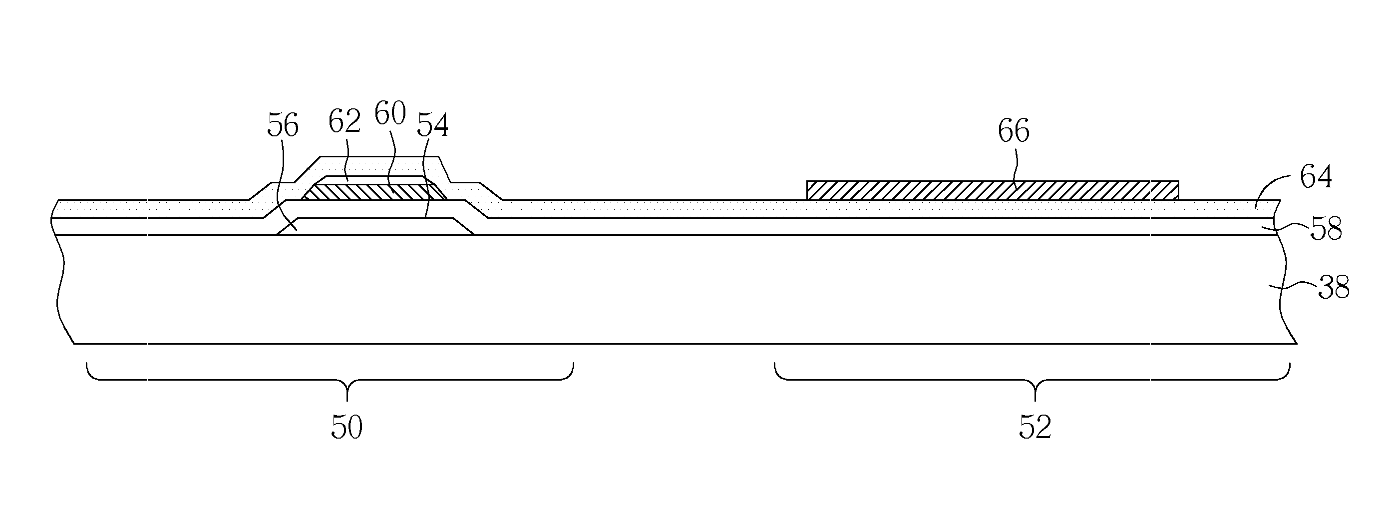
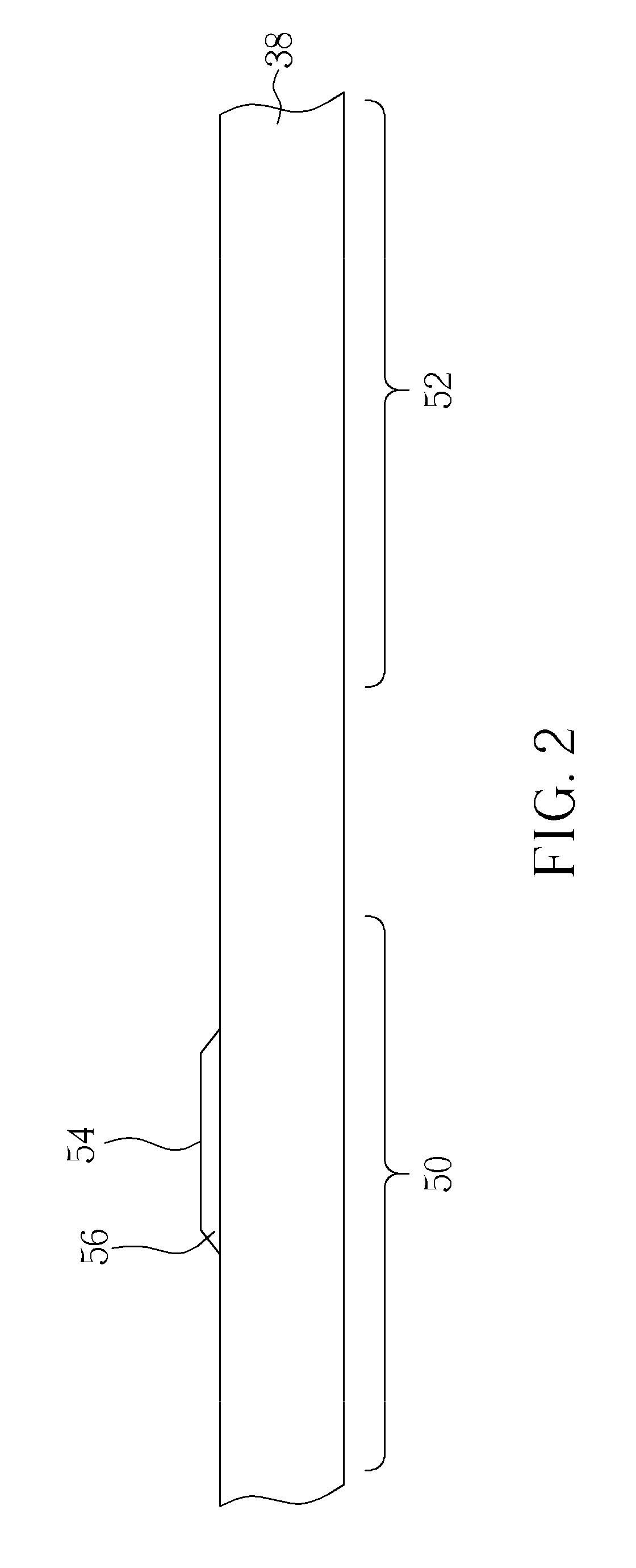
[0020]FIGS. 2-7 illustrate cross-sectional views of a method for forming a photo sensor on an amorphous silicon TFT display panel according to the present invention. As shown in FIG. 2, a substrate 38 is provided. The substrate 38, which may be an array substrate of a flat display panel, includes at least a TFT region 50, and at least a sensor region 52. A first conductive layer is then entirely deposited on the substrate 38, and a first photolithographic and etching process using a first mask is performed to form a first patterned conductive layer 54. The first pattern conductive layer 54 is preferably metal material, and includes a gate electrode 56 disposed in the TFT region 50. As shown in FIG. 3, a gate insulating layer 58 is deposited on the substrate 38 and the gate electrode 56, and an amorphous silicon layer and a doped amorphous silicon layer are consecutively formed on the gate insulating layer 58. A second photolithographic and etching process using a second mask is perf...

third embodiment

[0026]FIGS. 9-10 illustrate a method of forming a photo sensor according to the present invention, where FIG. 9 follows FIG. 3. As shown in FIG. 9, after forming the patterned amorphous silicon layer 60 and the doped amorphous silicon layer 62, a second patterned conductive layer 64′ including a source electrode 70, a drain electrode 72 and a bottom electrode 74 is formed on the substrate 38. The second patterned conductive layer 64′ may be formed by the following steps. First, a second conductive layer (as the second conductive layer 64 shown in FIG. 4) and a photoresist layer (not shown) are entirely deposited on the substrate 38. Then, a photolithographic and etching process is performed to partially remove the second conductive layer 64 and the doped amorphous silicon layer 62. Subsequently, a patterned passivation layer 78 including a through hole 80 partially exposing the drain electrode 72 and a through hole 92 exposing most of the bottom electrode 74 is formed on the substra...

fourth embodiment

[0028]In other embodiments of the present invention, the silicon-rich dielectric layer 66 is formed in the TFT region 50 as well as in the sensor region 52. FIG. 11 illustrates a method for forming a photo sensor according to the present invention, where FIG. 11 follows the fabrication of FIG. 9. As shown in FIG. 11, after forming the TFT 76 and the passivation layer 78, a patterned silicon-rich dielectric layer 66 is formed on the substrate 38. The silicon-rich dielectric layer 66 includes a first part 66a disposed in the sensor region 52, and a second part 66b disposed in the TFT region 50, where the first part 66a is used as the photosensitive material of the photo sensor 88, and the second part 66b is used as another passivation layer of the TFT 76, the source electrode 70 and the drain electrode 72. The patterned silicon-rich dielectric layer 66 may be formed by the following steps. First, a silicon-rich dielectric layer 66 is entirely deposited on the substrate 38. Then, a pho...


PUM

PropertyMeasurementUnit
conductiveaaaaaaaaaa
transparent conductiveaaaaaaaaaa
dielectricaaaaaaaaaa

Abstract

A method for fabricating a photo sensor on an amorphous silicon thin film transistor panel includes forming a photo sensor with a bottom electrode, a silicon-rich dielectric layer, and a top electrode, such that the light sensor has a high reliability. The fabrication method is compatible with the fabrication process of a thin film transistor.

Description

BACKGROUND OF THE INVENTION[0001]1. Field of the Invention[0002]The present invention relates to a method for fabricating a photo sensor on an amorphous silicon TFT panel, and more particularly, to a method for fabricating a photo sensor, which has a silicon-rich (Si-rich) dielectric layer, on an amorphous TFT panel.[0003]2. Description of the Prior Art[0004]Photo sensors have been widely used in various types of TFT displays. Currently, a photo sensor is normally a p-intrinsic-n (PIN) photodiode formed by IIIA material and VA material. The PIN photodiode, however, has low light receiving efficiency and tends to be influenced by untargeted light sources, and thus suffers disadvantages, e.g. poor signal-to-noise ratio. In addition, the IIIA material and VA material of the PIN photodiode and the TFT fabrication have compatibility problems, which limit the application and productivity of the traditional PIN photodiode. Recently, TFT sensors formed by amorphous silicon material have bee...

Claims


Application Information

Patent Timeline
Patent Type & Authority Patents(United States)
IPC IPC(8): H01L21/00
CPCH01L27/14692H01L31/095H01L27/1288
Inventor SHIH, CHING-CHIEHCHO, AN-THUNGPENG, CHIA-TIENLIN, KUN-CHIH
Owner OPTRONIC SCI LLC
Why Eureka
Try Eureka