Supercharge Your Innovation With Domain-Expert AI Agents!

Sequential storage circuitry for an integrated circuit

a technology of sequential storage circuit and integrated circuit, which is applied in the direction of electronic circuit testing, static storage, measurement devices, etc., can solve the problems of reducing the life of such devices, reducing the efficiency of sequential storage circuit, and increasing the cost of circuit overhead, so as to reduce the overhead of producing sequential storage circuits using the technique of the present invention. , the effect of de-stressing the downstream combinatorial logi

Active Publication Date: 2010-09-07
ARM LTD
View PDF3 Cites 3 Cited by
  • Summary
  • Abstract
  • Description
  • Claims
  • Application Information

AI Technical Summary

Benefits of technology

The present invention provides a sequential storage circuitry for an integrated circuit that includes input circuitry, a storage structure, and output circuitry. The input circuitry receives an input data value and generates an internal data value, which is either the input data value or an inverted version of it based on a first control signal. The storage structure stores an indication of the internal data value and the output circuitry generates an output data value based on the second control signal. The invention allows for the flipping of the stored data value periodically, even when the data input is static, to reduce stress on the storage structure. It provides a simple and effective mechanism to anneal stress in distributed sequential storage circuitry of an integrated circuit. The invention can be applied to sequential storage circuits distributed widely throughout the integrated circuit, without requiring modifications to other components of the integrated circuit. The first control signal is asserted before a predetermined edge of a clock signal, and the second control signal is generated responsive to the predetermined edge of the clock signal. The first and second control signals can be managed in various ways, such as by asserting them at different times or by using a flip-flop storage structure. The invention allows for the flipping of the stored data value without causing any changes to the output data value, and can be used to improve security of the data stored in the sequential storage circuitry. It provides a simple and effective mechanism to anneal stress in distributed sequential storage circuitry of an integrated circuit.

Problems solved by technology

The stress observed in the devices at these reduced geometries causes them to age faster, which reduces the life of such devices.
NBTI is an effect that primarily affects the PMOS devices, causing them to become stressed at higher temperature when the gate-source bias is negative.
The usual impact of NBTI is an increase in the device threshold (Vt) over the life of the device, which slows the operation of the device down as it ages with use.
Hence, the degradation of device threshold can manifest as path delay failures in the device.
However, any low activity domains are under much more stress due to almost static bias.
If the static stress remains for a substantially long time, even a subsequent change in bias cannot recover the Vt degradation.
Over-design with margins has become very expensive due to stringent area, performance and power demands for nanometer designs.
However, every gate has a different optimal ratio and it is not possible to have an independent supply for every gate.Gate sizing: This involves increasing the device size and over-design.
However, as mentioned earlier, this has significant costs in terms of area and power.Stack effect: This involves replacing a transistor with two or more transistors in series (a “stack”), which increases Vt due to the body effect.
This hence reduces the effect of Vt degradation over time due to NBTI, but with a performance cost resulting from the use of stacked transistors.Duty cycle control: This involves reducing the proportion of time that the gate of a PMOS device is at a logic “0” voltage level, which can reduce Vt degradation due to NBTI.
All of the techniques mentioned above are expensive to implement, either due to area increase, power increase, increase in complexity of the overall system design, or a combination of these factors.
The same technique cannot be used for sequential storage circuitry such as flip-flops and latches, or for the combinatorial circuitry interposed between such sequential storage circuitry, due to their spatial distributions on chip.

Method used


Image

  • Sequential storage circuitry for an integrated circuit
  • Sequential storage circuitry for an integrated circuit
  • Sequential storage circuitry for an integrated circuit

Examples


Embodiment Construction

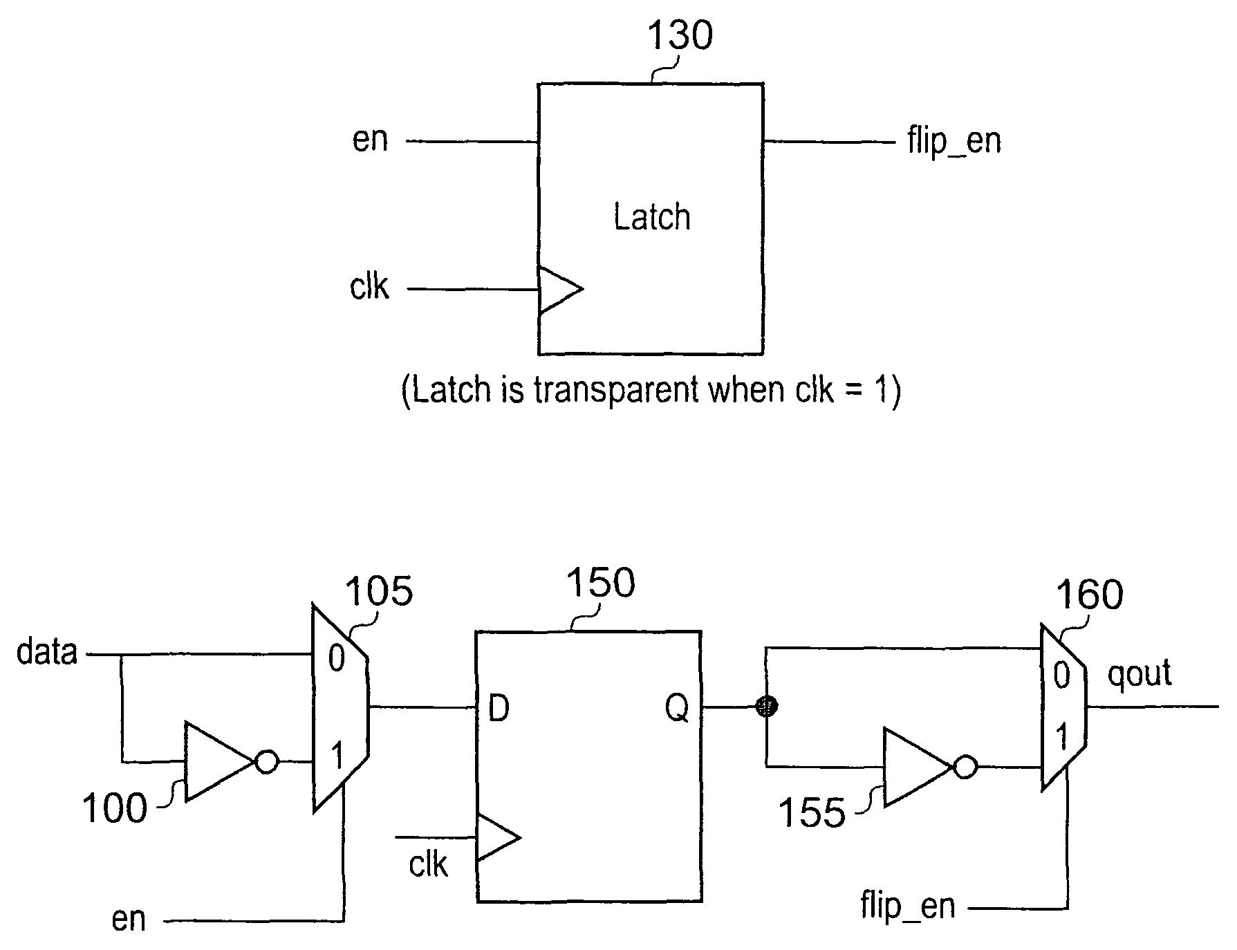
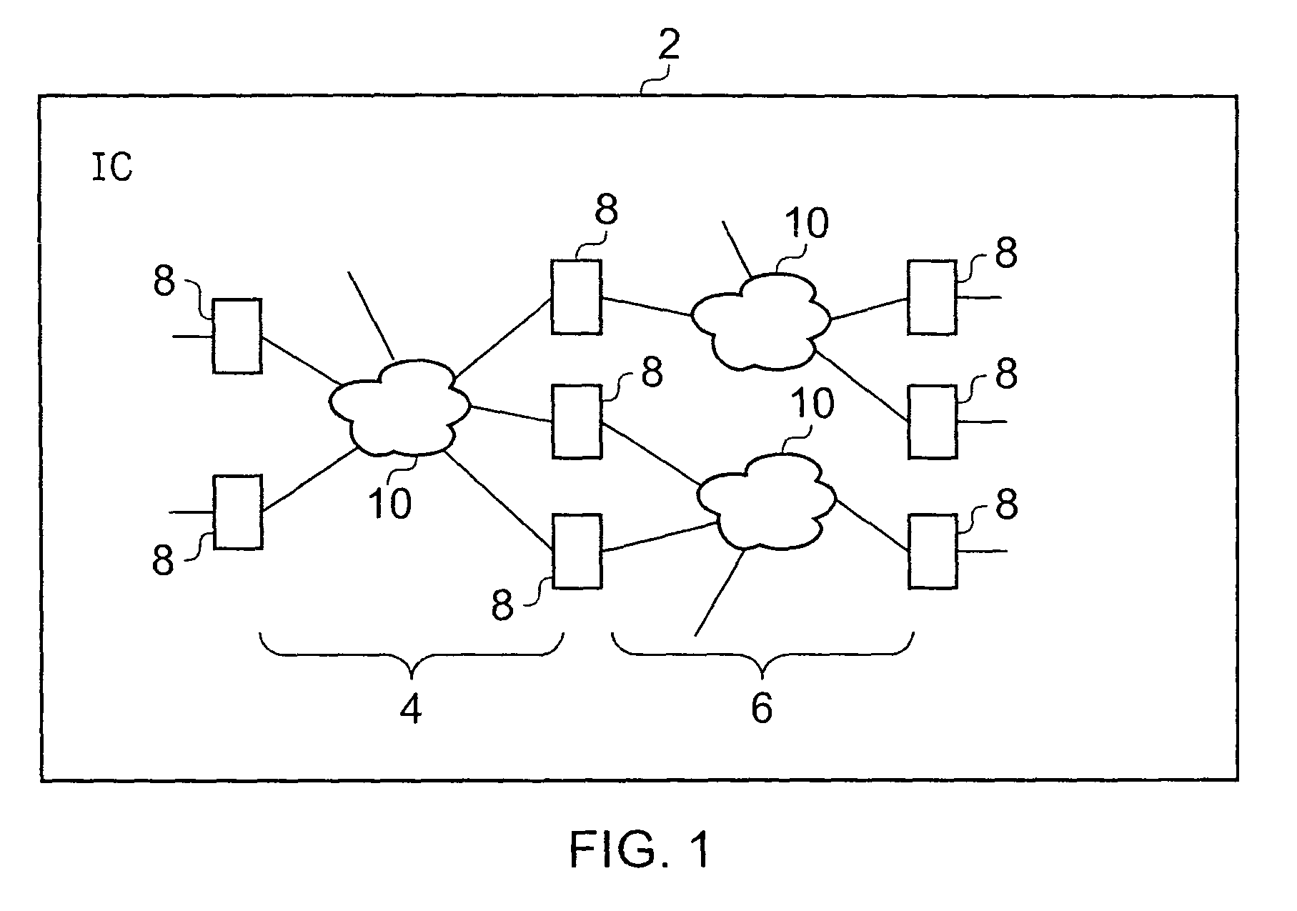
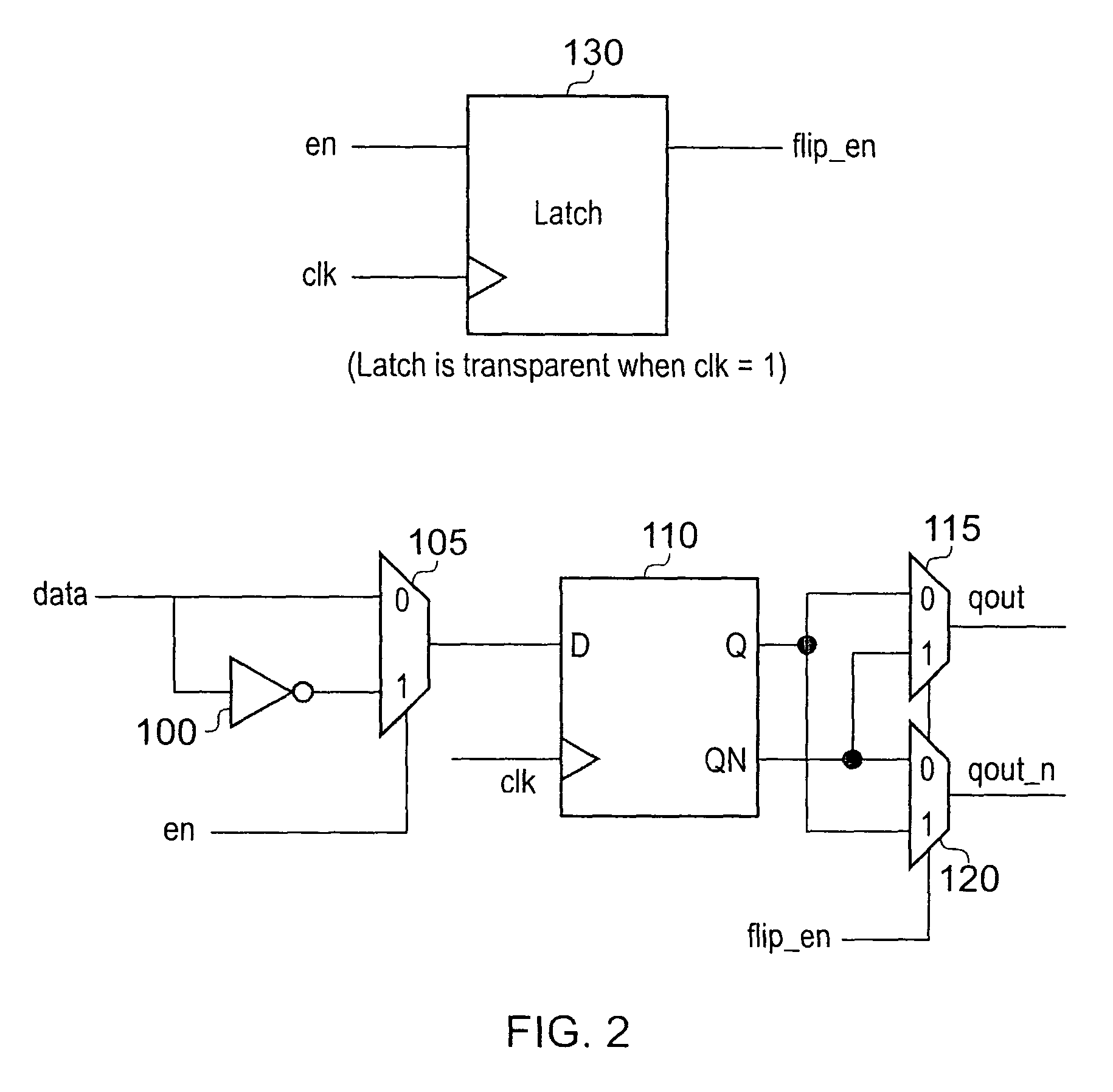
[0046]FIG. 1 shows an integrated circuit 2 including pipeline stages 4, 6 extending between sequential storage circuitry 8 which may be in the form of flip-flops or latches. Between the sequential storage circuits 8 are respective instances of combinatorial logic circuitry 10, which serve to receive signals from one or more preceding stages and generate signals to be passed to one or more succeeding stages. The period of time between the capture of signal values by the sequential storage circuits 8 for successive clock periods is the time that is available for the combinatorial logic circuitry 10 to evaluate its inputs so as to generate its outputs. Embodiments of the present invention provide a new design for the sequential storage circuit 8, which can serve to anneal stress build-up within the sequential storage circuit, and / or be used to improve security of the data stored therein.

[0047]For the purposes of discussing the following embodiments of the present invention, it will be ...


PUM


Abstract

Sequential storage circuitry is provided for an integrated circuit, comprising input circuitry, a storage structure, and output circuitry. The input circuitry receives an input data value to the sequential storage circuitry, and generates an internal data value. The input circuitry receives a first control signal which when asserted causes it to generate as the internal data value an inverted version of the input data value, and which when not asserted causes the input circuitry to generate as the internal data value the input data value. The storage structure then stores an indication of the internal data value. The output circuitry generates, from the indication of the internal data value stored in the storage structure, an output data value for outputting from the sequential storage circuitry. More particularly, the output circuitry receives a second control signal derived from the first control signal, which causes the output circuitry to generate as said output data value an inverted version of the internal data value in the event that the input circuitry generated as the internal data value an inverted version of the input data value, and otherwise generates as the output data value the internal data value.

Description

BACKGROUND OF THE INVENTION[0001]1. Field of the Invention[0002]The present invention relates to sequential storage circuitry for an integrated circuit.[0003]2. Description of the Prior Art[0004]As device geometries shrink (for example there is currently much development in the area of sub-45 nm technology design), this has pushed existing CMOS materials much closer to their intrinsic reliability limits. The stress observed in the devices at these reduced geometries causes them to age faster, which reduces the life of such devices. Many articles have been written concerning this reliability problem, see for example the article “Designing Reliable Systems from Unreliable Components: The Challenges of Transistor Variability and Degradation”, by S Borkar, IEEE Micro November-December 2005, and the article “Reliability Challenges for 45 nm and Beyond” by J McPherson, IEEE Design Automation Conference (DAC), 2006. The reliability problem is often touted as one of the most important conce...

Claims


Application Information

Patent Timeline
Patent Type & Authority Patents(United States)
IPC IPC(8): G01R31/28
CPCG11C8/04
Inventor CHANDRA, VIKASIDGUNJI, SACHIN SATISH
Owner ARM LTD
Features
  • R&D
  • Intellectual Property
  • Life Sciences
  • Materials
  • Tech Scout
  • Unparalleled Data Quality
  • Higher Quality Content
  • 60% Fewer Hallucinations
Learn More