PLL circuit and semiconductor device having the same

a technology of semiconductor devices and circuits, applied in the direction of pulse automatic control, pulse generation by logic circuits, pulse techniques, etc., can solve the problems of unstable input signal of vco, difficult to maintain stable control operation, unstable operation of pll circuits, etc., to achieve short lock time, short lock time, and longer lock time

Inactive Publication Date: 2010-09-21
SEMICON ENERGY LAB CO LTD
View PDF9 Cites 5 Cited by
  • Summary
  • Abstract
  • Description
  • Claims
  • Application Information

AI Technical Summary

Benefits of technology

[0006]Thus, it is an object of the invention to reduce the interval from the time when a signal is input to a PLL circuit until it generates an arbitrary frequency. It is another object of the invention to provide a PLL circuit which can operate in a stable manner and a semiconductor device having the same.
[0013]When priority is given to the property of the LP whereby high frequency components are removed from output signals of the phase detector, the lock time becomes longer; however, when the VCO is operated stably with a free-running oscillation at a desired frequency with the use of the output current Iout of a current source, a stable PLL circuit with short lock time can be realized.
[0014]According to the invention, a PLL circuit with short lock time can be realized by using a variable frequency oscillator (VCO). Furthermore, the PLL circuit can be operated stably.

Problems solved by technology

If the lock time is short, the control operation can be performed in a short time after a signal input; however, since the operation is adversely affected in the case where the input signal has noise, it is difficult to maintain stable control operation.
Therefore, when a switch circuit is provided, an input signal of the VCO becomes unstable when it is mixed with noise or the like, and this will be a factor which makes the operation of the PLL circuit unstable.
As a result, it is necessary to wait until the conditions for a stable free-running oscillation are obtained, and in such a case, it makes no sense to provide a switch circuit in order to reduce the lock time.

Method used


Image

  • PLL circuit and semiconductor device having the same
  • PLL circuit and semiconductor device having the same
  • PLL circuit and semiconductor device having the same

Examples


embodiment mode 1

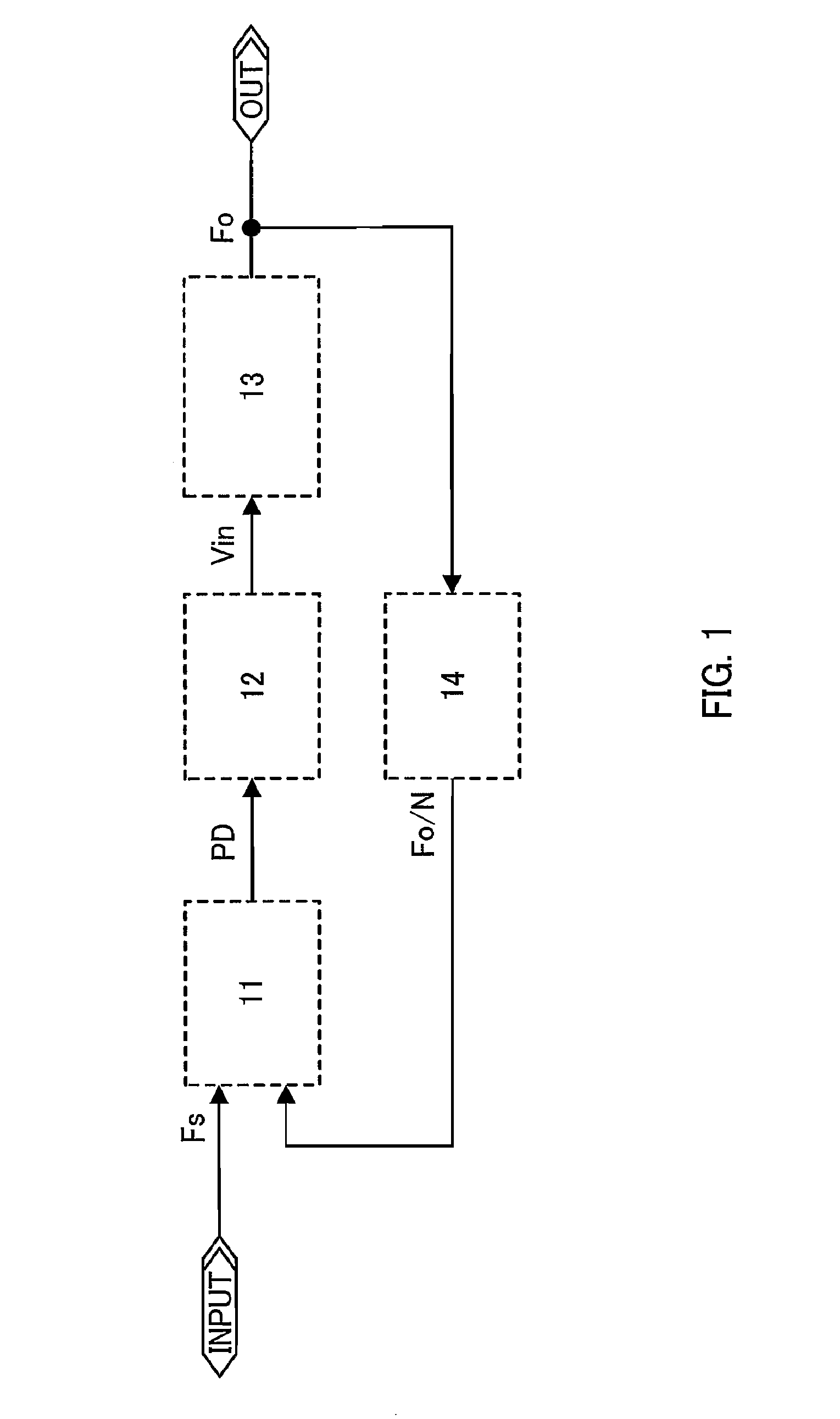
[0030]FIG. 1 shows a block diagram of a PLL circuit in accordance with this embodiment mode. The PLL circuit includes a phase detector 11, a loop filter (LF)12, a voltage-controlled oscillator (VCO) 13, and a frequency divider 14. The phase detector 11 compares a phase of a signal Fs which is input from outside with a phase of a signal Fo / N which is input from the frequency divider 14. The loop filter 12 generates a signal Vin by removing alternating current components from a signal input from the phase detector 11. The voltage-controlled oscillator 13 outputs a signal Fo based on the signal Vin input from the loop filter 12. The frequency divider 14 converts the signal Fo output from the voltage-controlled oscillator 13 into Fo / N (frequency division by N), and outputs it to the phase detector 11.

[0031]Note that the PLL circuit in accordance with this embodiment mode is required to have at least the voltage-controlled oscillator 13. The phase detector 11, the loop filter 12, and the...

embodiment mode 2

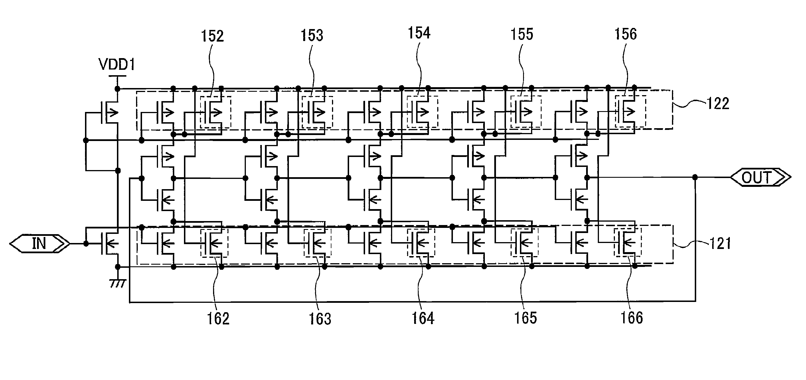
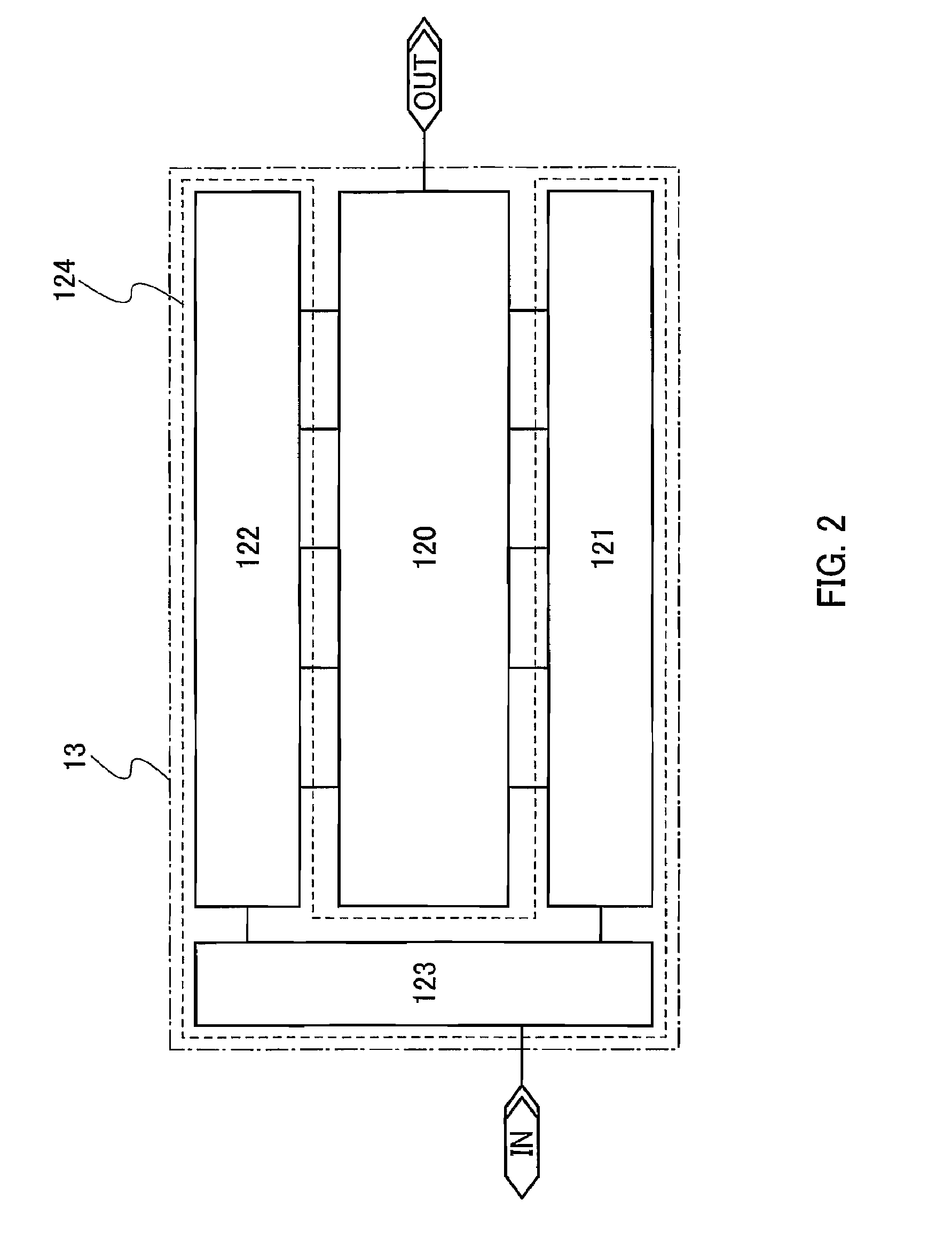
[0054]In this embodiment mode, a configuration of a unit circuit 21 (exclusive OR circuit) of the phase detector 11 is described with reference to FIG. 7. The unit circuit 21 includes a NOR circuit 221 and transistors 222 to 227. In addition, the unit circuit 21 has two input terminals (indicated by 1 and 2 in FIG. 7), and one output terminal (indicated by 3 in FIG. 7).

[0055]This unit circuit 21 operates in the following manner. Upon input of the same signals to the input terminal 1 and the input terminal 2, an H-level signal is output from the output terminal 3. Upon input of different signals to the input terminal 1 and the input terminal 2, an L-level signal is output from the output terminal 3. That is, the unit circuit 21 compares a phase of a signal input to the input terminal 1 with a phase of a signal input to the input terminal 2, and outputs a signal from the output terminal 3 based on the result of the comparison.

[0056]Next, a configuration of a unit circuit 26 of the fre...

embodiment mode 3

[0059]FIG. 9 shows a configuration of a semiconductor device in accordance with this embodiment mode. This semiconductor device 300 includes an antenna 301, a modulation circuit 307, a rectifier circuit 302, a demodulation circuit 303, a signal processing circuit 306, a memory 305, and a PLL circuit 304. The PLL circuit 304 has a similar configuration to Embodiment Mode 1. Signals which are transmitted from a reader device to this semiconductor device 300 are received at the antenna 301. One of the signals is used for generating power in the rectifier circuit 302. Modulated signals are demodulated in the demodulation circuit 303, and the demodulated signals are input into the PLL circuit 304. Then, the PLL circuit 304 generates clocks in synchronization with the demodulated signals. The signal processing circuit 306 processes the demodulated signals by using the clocks, and then sends the processed signals back to the modulation circuit 307.

[0060]The semiconductor device 300 in acco...


PUM


Abstract

A PLL circuit includes a phase detector, a loop filter (LF), a voltage-controlled oscillator (VCO), and a frequency divider. The phase detector compares a phase of a signal Fs which is input from outside with a phase of a signal Fo / N which is input from the frequency divider. The loop filter generates a signal Vin by removing alternating current components from a signal input from the phase detector. The voltage-controlled oscillator outputs a signal Fo based on the signal Vin input from the loop filter. The frequency divider converts the signal Fo output from the voltage-controlled oscillator into Fo / N (frequency division by N), and outputs it to the phase detector.

Description

TECHNICAL FIELD[0001]The present invention relates to a PLL circuit and a semiconductor device having the same.BACKGROUND ART[0002]Conventionally, a phase-locked loop circuit (hereinafter referred to as a PLL circuit) has been known as a circuit which generates clocks with an arbitrary synchronous frequency with input signals.[0003]A PLL circuit is mounted with a variable frequency oscillator, and compares a phase of an input signal with that of a feedback signal output from the oscillator. The PLL circuit performs negative feedback control so that the input signal is synchronized with the feedback signal (i.e., to maintain a fixed phase relationship between the input signal and the feedback signal). This control operation is called locking (also called phase locking). In addition, the time required for such control operation is called lock time (also called phase-lock time).[0004]Lock time is generally determined by the time constant of a loop filter in a PLL circuit. If the time c...

Claims


Application Information

Patent Timeline
Patent Type & Authority Patents(United States)
IPC IPC(8): H03B27/00
CPCH03K3/014H03K3/0315H03L7/099H03L7/0995H03L7/085
Inventor KOYAMA, JUNOSADA, TAKESHI
Owner SEMICON ENERGY LAB CO LTD
Why Eureka
Try Eureka