Physical-resist model using fast sweeping

a fast sweep and resist technology, applied in the field of modeling resist development, can solve the problems of determining the necessary photo-mask modification used in these techniques, accompanied by unwanted distortions and artifacts, and becoming time-consuming and expensiv

Inactive Publication Date: 2010-09-28
DINO TECH ACQUISITION
View PDF0 Cites 34 Cited by
  • Summary
  • Abstract
  • Description
  • Claims
  • Application Information

AI Technical Summary

Problems solved by technology

Unfortunately, due to the wave nature of light, as the dimensions approach length scales comparable to the wavelength of the light used in the photolithography process, the resulting wafer patterns deviate from the corresponding photo-mask patterns and are accompanied by unwanted distortions and artifacts.
However, determining the necessary photo-mask modifications used in these techniques, which is often determined by trial and error, is increasingly time consuming and expensive.
Unfortunately, existing models of the resist-development process are often complicated.
When these calculations are repeated multiple times, such as in an iterative ILT or OPC calculation, there may be a prohibitive increase in the overall calculation time.

Method used


Image

  • Physical-resist model using fast sweeping
  • Physical-resist model using fast sweeping
  • Physical-resist model using fast sweeping

Examples


Embodiment Construction

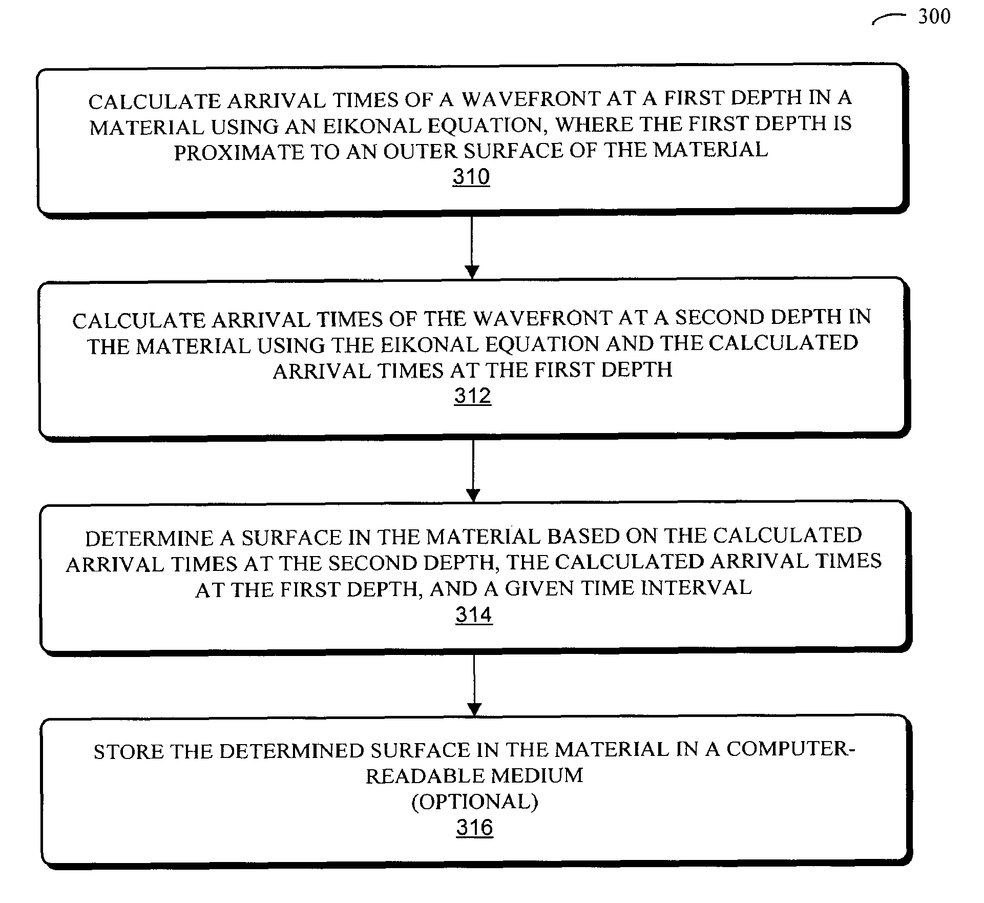
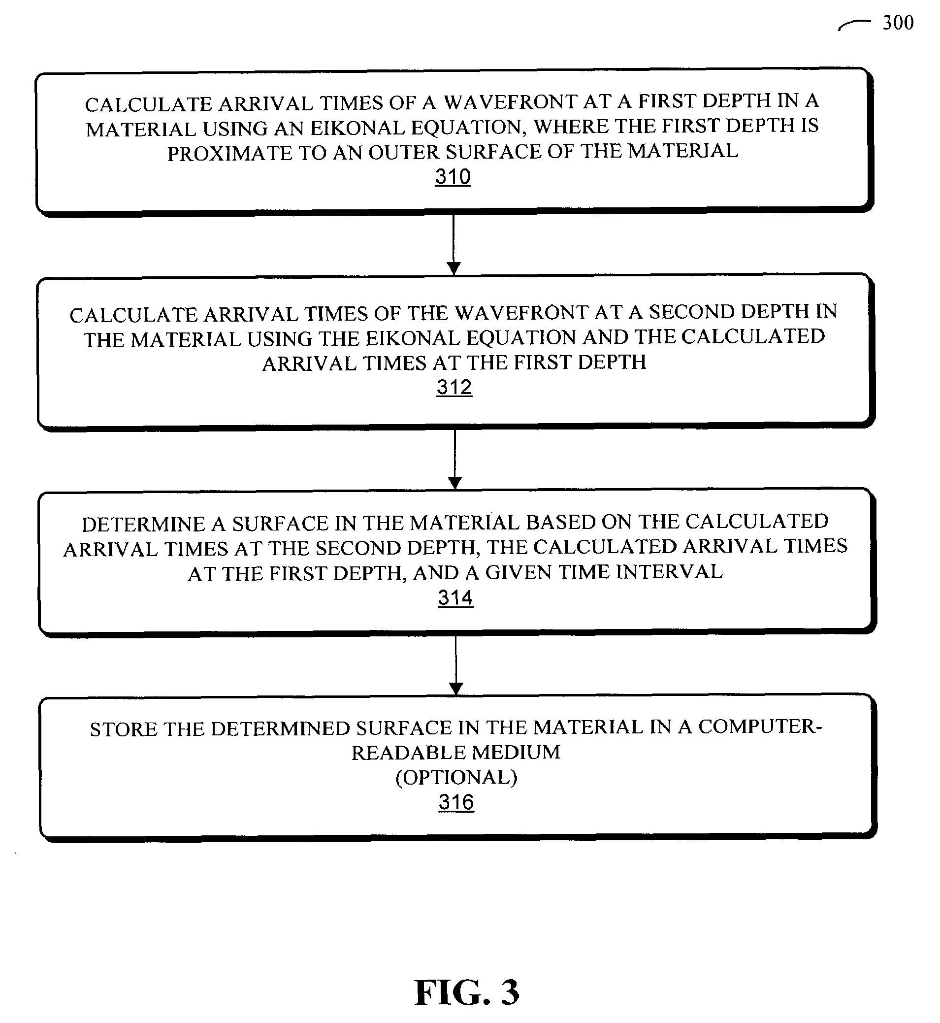
[0031]The following description is presented to enable any person skilled in the art to make and use the invention, and is provided in the context of a particular application and its requirements. Various modifications to the disclosed embodiments will be readily apparent to those skilled in the art, and the general principles defined herein may be applied to other embodiments and applications without departing from the spirit and scope of the present invention. Thus, the present invention is not intended to be limited to the embodiments shown, but is to be accorded the widest scope consistent with the principles and features disclosed herein.

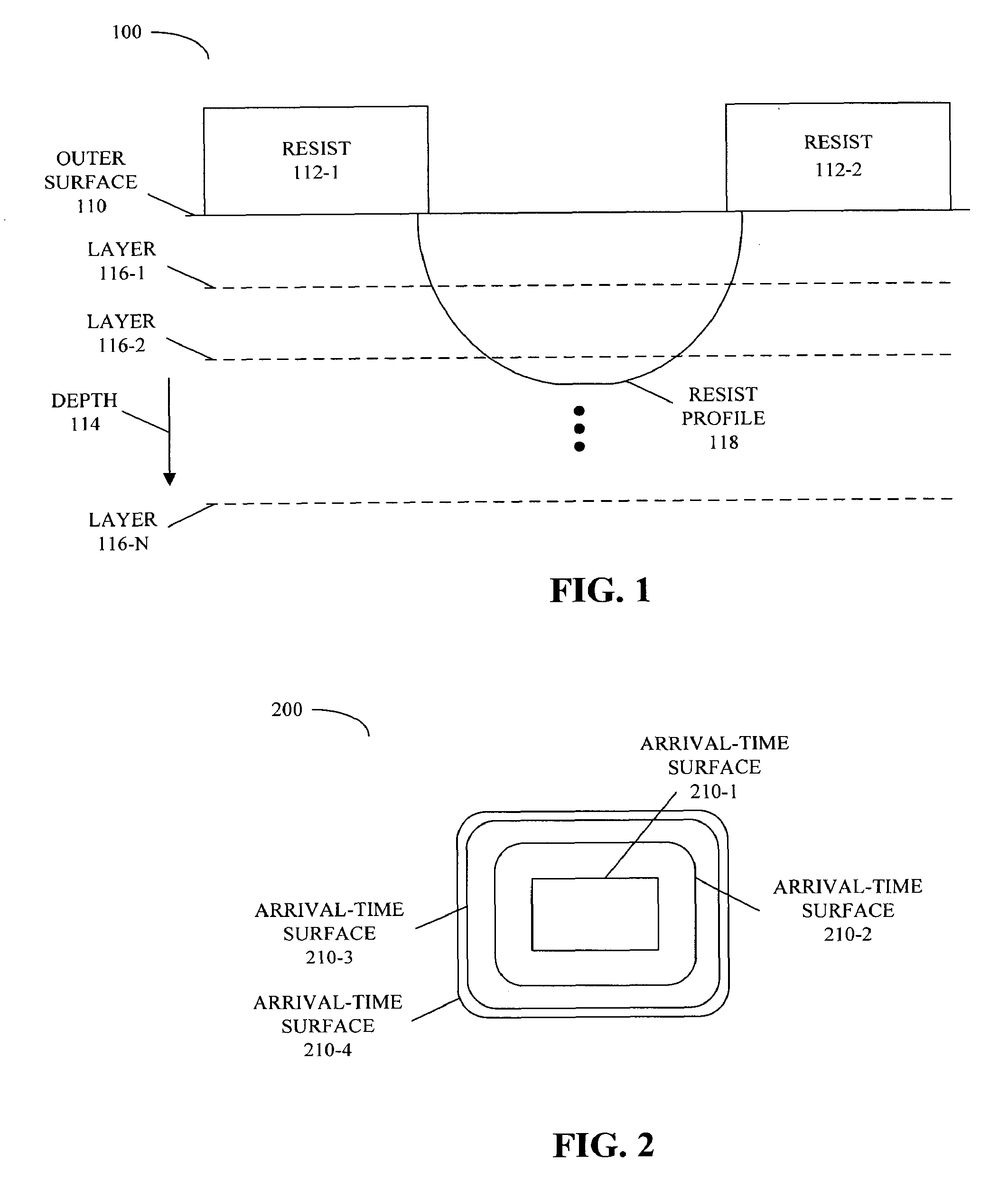
[0032]Embodiments of a computer system, a method, and a computer program product (i.e., software) for use with the computer system are described. These systems and processes may be used to model at least a portion of a (photo-) lithographic processes and / or semiconductor-manufacturing processes. These processes may include photo-masks that prin...


PUM


Abstract

A method for determining a surface in a material is described. During this method, arrival times of a wavefront at a first depth in the material are calculated using an Eikonal equation. Note that the first depth is proximate to an outer surface of the material. Next, arrival times of the wavefront at a second depth in the material are calculated using the Eikonal equation and the calculated arrival times at the first depth. Then, the surface in the material is determined based on the calculated arrival times at the first depth, the calculated arrival times at the second depth, and a given time interval. Note that arrival times at a given depth in the material, which includes the first depth or the second depth, are calculated by directly determining a steady-state solution of the Eikonal equation.

Description

FIELD OF THE INVENTION[0001]The present invention relates to techniques for modeling resist development in lithographic processes that use photo-masks and semiconductor-manufacturing processes that use direct-write devices.BACKGROUND[0002]Lithography processing represents an essential technology for manufacturing Integrated Circuits (IC) and Micro Electro-Mechanical Systems (MEMS). In these processes, lithographic techniques are used to define patterns, geometries, features, shapes, etc. onto an integrated circuit die or semiconductor wafer or chips. For example, a photo-mask may be used to print a pattern in a layer on a semiconductor wafer that is subsequently developed to produce a feature. However, in other techniques a device may directly write the pattern, for example, using an electron beam or a laser beam.[0003]As the density of features on the dies and wafers has increased, the minimum dimension (also known as the critical dimension) in the designs has decreased. Unfortunat...

Claims


Application Information

Patent Timeline
Patent Type & Authority Patents(United States)
IPC IPC(8): G06F17/50
CPCG03F1/144G03F1/36G03F7/705
Inventor PENG, DANPING
Owner DINO TECH ACQUISITION
Why Eureka
Try Eureka