Silicon carbide semiconductor device

a silicon carbide and semiconductor technology, applied in the direction of semiconductor devices, basic electric elements, electrical appliances, etc., can solve the problems of difficult to form a p type, difficult to absorb surge energy, and difficult diffusion process widely used in silicon device manufacturing, etc., to achieve the effect of improving the surge resistan

Inactive Publication Date: 2010-10-05
DENSO CORP
View PDF31 Cites 14 Cited by
  • Summary
  • Abstract
  • Description
  • Claims
  • Application Information

AI Technical Summary

Benefits of technology

[0009]In view of the above and other difficulties, it is an objective of the present invention to provide a silicon carbide semiconductor device having a vertical type semiconductor element capable of improving a surge resistance.
[0011]According to the above silicon carbide semiconductor device, due to a presence of the above first conductivity type region, a breakdown occurs at a corner part of the first conductivity type region on an upper side. The first conductivity type region causes a body breakdown to occur. Accordingly, it is possible to improve a surge resistance.
[0013]According to the above silicon carbide semiconductor device, due to a presence of the above first conductivity type region, a breakdown occurs at a corner part of the first conductivity type region on an upper side. The first conductivity type region causes a body breakdown to occur. Accordingly, it is possible to improve a surge resistance.
[0015]According to the above silicon carbide semiconductor device, due to a presence of the above first conductivity type region, a breakdown occurs at a corner part of the first conductivity type region on an upper side. The first conductivity type region causes a body breakdown to occur. Accordingly, it is possible to improve a surge resistance.
[0017]According to the above silicon carbide semiconductor device, due to a presence of the above first conductivity type region, a breakdown occurs at a corner part of the first conductivity type region on an upper side. The first conductivity type region causes a body breakdown to occur. Accordingly, it is possible to improve a surge resistance. Since the first conductivity type region is certainly located lower than the second conductivity type region, an avalanche breakdown can take place in the cell portion. Accordingly, it is possible to improve a surge resistance.
[0019]According to the above silicon carbide semiconductor device, due to a presence of the above first conductivity type region, a breakdown occurs at a corner part of the first conductivity type region on an upper side. The first conductivity type region causes a body breakdown to occur. Accordingly, it is possible to improve a surge resistance.

Problems solved by technology

In manufacturing an SiC semiconductor device, since impurities are difficult to diffuse in SiC, it is difficult to employ a diffusion process that is widely used in manufacturing a silicon device.
It is hence difficult to form a p type well layer to a deep position in SiC by the diffusion process.
Since an area of the periphery of the cell portion is relatively small, a surge energy is difficult to be absorbed.
Alternatively, the p type base region may be biased, and a substrate bias effect may non-uniformly form a channel and cause element destruction.

Method used


Image

  • Silicon carbide semiconductor device
  • Silicon carbide semiconductor device
  • Silicon carbide semiconductor device

Examples


first embodiment

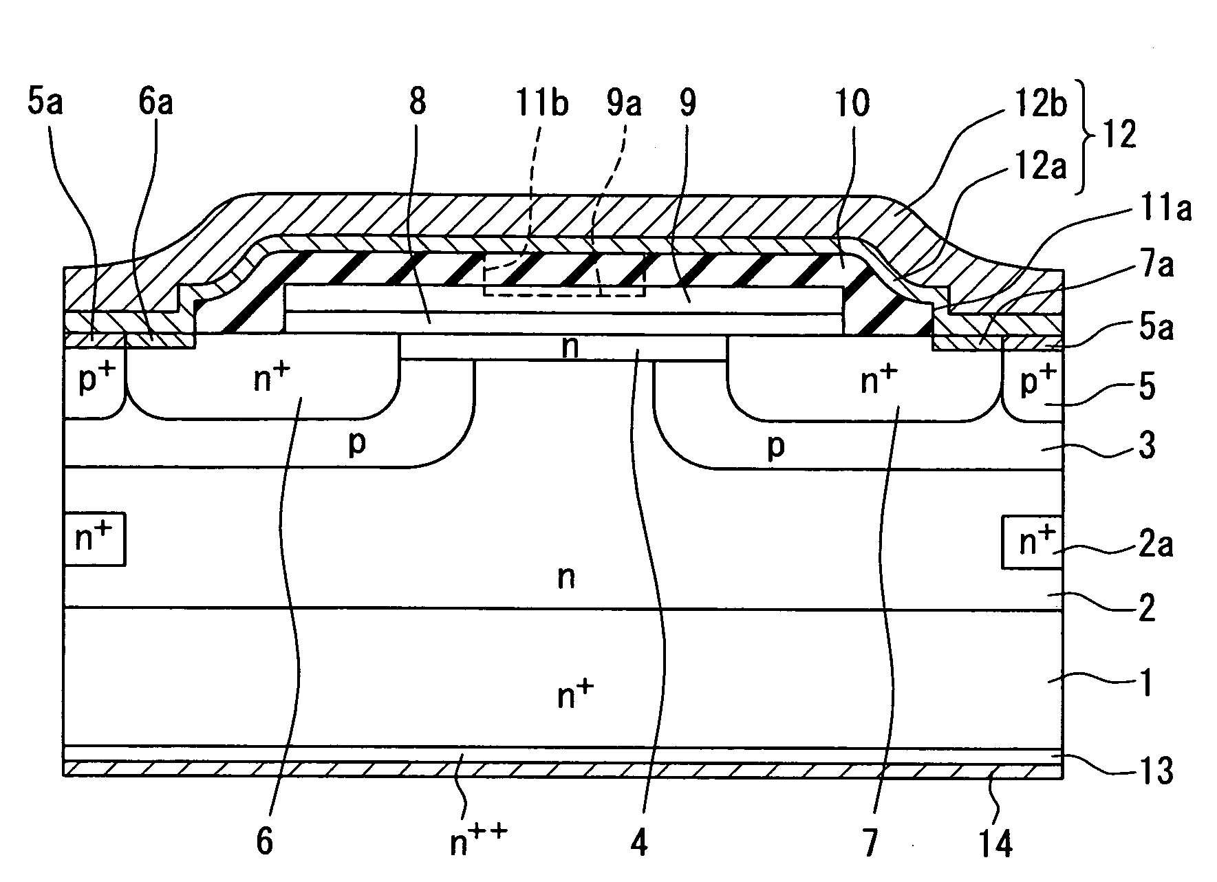
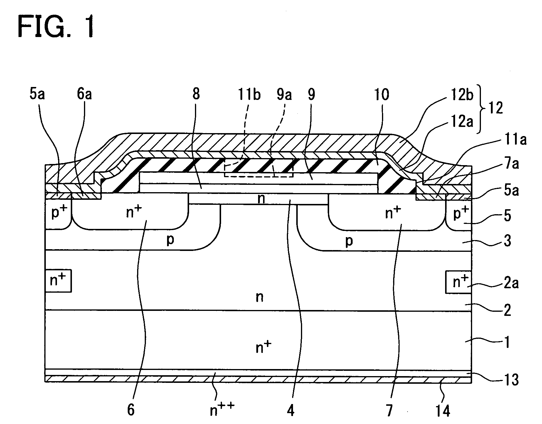
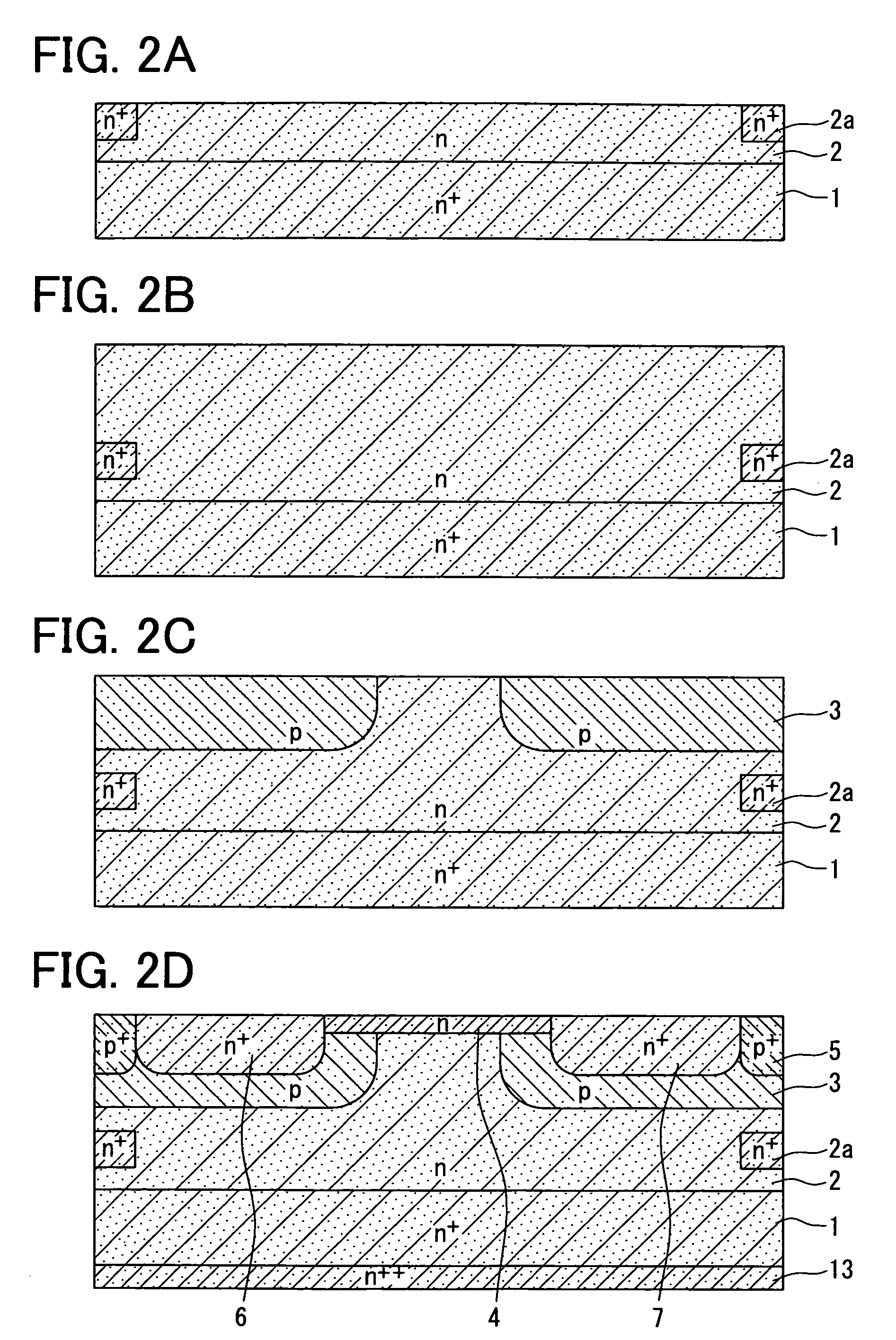
[0035]A first embodiment is explained below. In the present embodiment, an SiC semiconductor device including a planer MOSFET is presented. A configuration of the planer MOSFET and a method of manufacturing the planer MOSFET are described below with reference to FIG. 1, FIGS. 2A to 2D, and FIGS. 3A to 3D. FIG. 1 is a cross sectional diagram illustrating the SiC semiconductor device having the planer MOSFET in accordance with the present embodiment. FIGS. 2A to 2D and FIG. 3A to 3D are cross sectional diagrams illustrating manufacturing processes of the planer MOSFET shown in FIG. 1.

[0036]As shown in FIG. 1, the planer MOSFET is formed by using a substrate 1. The substrate 1 is made of SiC, having an n+ conductivity type, and having a principal surface on one surface side. For example, the substrate 1 is made of 4H-SiC and have an impurity concentration of about 5×1018 cm−3. The substrate 1 has the principal surface on a-face, for example, on the (11-20) face.

[0037]An n type drift la...

second embodiment

[0064]A second embodiment is described below. An SiC semiconductor device having a planer MOSFET according to the present embodiment is different from that according to the first embodiment in a location of n+ type region 2a.

[0065]FIG. 4 is a cross sectional diagram illustrating the SiC semiconductor device having the planer MOSFET in accordance with the present embodiment. As shown in FIG. 4, each n+ type region 2a is located in the n type drift layer 2, located below the n+ type source region 6, 7, and spaced away from the p type base region 3. Functions of the n+ type regions 2a according to the present embodiment are substantially identical those according to the first embodiment. Effects according to the present embodiment are substantially similar to those according to the first embodiment.

[0066]A method for manufacturing the planer MOSFET according to present embodiment is provided when the following change is made in the method according to the first embodiment. The change ...

third embodiment

[0067]A third embodiment is described below. An SiC semiconductor device having a planer MOSFET according to the present embodiment is different from that according to the first embodiment in a location of an n+ type region 2a.

[0068]FIG. 5 is a cross sectional diagram illustrating the SiC semiconductor device having the planer MOSFET in accordance with the present embodiment. As shown in FIG. 5, each n+ type region 2a is located in the n type drift layer 2, and located below the contact region 5, as similar to the n+ type region 2a according to the first embodiment. In the present embodiment, the n+ type region 2a is in contact with the substrate 1 whereas, in the first embodiment, the n+ type region 2a is spaced away from the substrate 1. Functions of the n+ type regions 2a contacting the substrate 1 according to the present embodiment includes those according to the first embodiment. Effects according to the present embodiment include those according to the first embodiment. More...


PUM

PropertyMeasurementUnit
thicknessaaaaaaaaaa
thicknessaaaaaaaaaa
thicknessaaaaaaaaaa

Abstract

A silicon carbide semiconductor device is disclosed. The silicon carbide semiconductor device includes a substrate; a drift layer having a first conductivity type and located on a first surface of the substrate; and a vertical type semiconductor element. The vertical type semiconductor element includes: an impurity layer having a second conductivity type, and located in a surface portion of the drift layer; and a first conductivity type region located in the drift layer, spaced away from the impurity layer, located closer to the substrate than the impurity layer, and having an impurity concentration higher than the drift layer.

Description

CROSS REFERENCE TO RELATED APPLICATION[0001]The present application is based on Japanese Patent Application No. 2007-262031 filed on Oct. 5, 2007, the disclosure of which is incorporated herein by reference.BACKGROUND OF THE INVENTION[0002]1. Field of the Invention[0003]The present invention relates to a silicon carbide semiconductor device.[0004]2. Description of Related Art[0005]A silicon carbide semiconductor device is a device that is formed by using silicon carbide (SiC) as semiconductor material. JP-A-H10-308510, corresponding to U.S. Pat. No. 6,573,534, discloses an SiC semiconductor device including a planer metal-oxide-semiconductor field-effect transistor (MOSFET). JP-A-H5-55594 discloses a configuration for improving a surge resistance of a silicon semiconductor device. According to the configuration, a p type well region that functions as a deep base region is located below a p type base region.[0006]The inventors have revealed the following idea, as a related art. A sur...

Claims


Application Information

Patent Timeline
Patent Type & Authority Patents(United States)
IPC IPC(8): H01L29/15H01L31/0312
CPCH01L29/0847H01L29/0878H01L29/6606H01L29/66068H01L29/7813H01L29/7828H01L29/861H01L29/872H01L29/0615H01L29/0619H01L29/0623H01L29/0692H01L29/1608H01L29/45H01L29/7395H01L29/7397H01L29/7802H01L29/8083
Inventor ENDO, TAKESHIOKUNO, EIICHI
Owner DENSO CORP
Why Eureka
Try Eureka