Coating and developing apparatus, coating and developing method and storage medium in which a computer-readable program is stored

a technology of developing apparatus and computer program, applied in the direction of resistive material coating, metallic material coating process, electric digital data processing, etc., can solve the problems of increasing the cost, affecting the uniformity of the line width of the circuit pattern, and affecting the resolution of the resist pattern just below such sites, so as to reduce the adverse effect of resist pattern resolution, reduce the number of heating sections, and reduce the effect of throughput control

Active Publication Date: 2010-10-05
TOKYO ELECTRON LTD
View PDF7 Cites 10 Cited by
  • Summary
  • Abstract
  • Description
  • Claims
  • Application Information

AI Technical Summary

Benefits of technology

[0016]It is another object of the present invention to provide a technique for providing a periphery exposing process to a substrate which has been subjected to a dipping exposure process as well as for adjusting the time taken from the end of the exposure to start of a heating process.
[0032]Liquid drops attached onto a substrate will become smaller in size quite rapidly after some period of time has elapsed after the attachment, thus degenerated layers (water marks) are formed in a resist film on the substrate. The present invention addresses this problem, and is hence constructed to control conveyance of each substrate such that it can be washed in a washing section in a period of time prior to a time zone in which the size of liquid drops becomes smaller quite rapidly. Accordingly, the occurrence of degenerated layers of the resist film can be controlled, thereby suppressing adverse effect on resolution of the resist pattern due to remaining water drops.
[0033]According to the present invention, the time to be taken from washing a substrate having been subjected to a dipping exposure process, through providing a periphery exposing process to the substrate, to heating the substrate after being subjected to the dipping exposure can be adjusted among wafers. Specifically, the time to be taken from a point of time the washing of each substrate in a washing section starts to a point of time the substrate is carried into a periphery exposing section can be set at a predetermined time. Accordingly, when the substrate is carried out from the periphery exposing section, the time elapsed after the dipping exposure process is approximately equal among wafers. Therefore, by carrying each substrate having been subjected to the periphery exposing process into the heating section in preference to other carrying works, the time elapsed described above can be adjusted among wafers and also the reduction of throughput can be controlled. In the case where the adjustment of the time elapsed from the dipping exposure to the heating process is performed in the heating section, the time of stay for each wafer in the heating section becomes longer, thus the number of heating sections should be increased. However, according to the present invention, the number of heating sections can be reduced.

Problems solved by technology

In such a case, when heating is provided to the wafer W after exposure, if water drops exist on the wafer, the temperature at sites on which the water drops remain becomes different from other regions, leading to causing an adverse effect on the pattern resolution just below such sites.
In such a case, uniformity of the line width of the circuit pattern will be adversely affected.
However, since the protective film tends to be damaged upon the periphery exposing process, it has been examined to perform the periphery exposing process after a wafer to be processed is returned from the exposing apparatus to the coating and developing apparatus.
However, in the method of performing the adjustment of the PED time by using the cooling plate, the number of heating sections becomes large, leading to increase of the cost.

Method used


Image

  • Coating and developing apparatus, coating and developing method and storage medium in which a computer-readable program is stored
  • Coating and developing apparatus, coating and developing method and storage medium in which a computer-readable program is stored
  • Coating and developing apparatus, coating and developing method and storage medium in which a computer-readable program is stored

Examples


examples

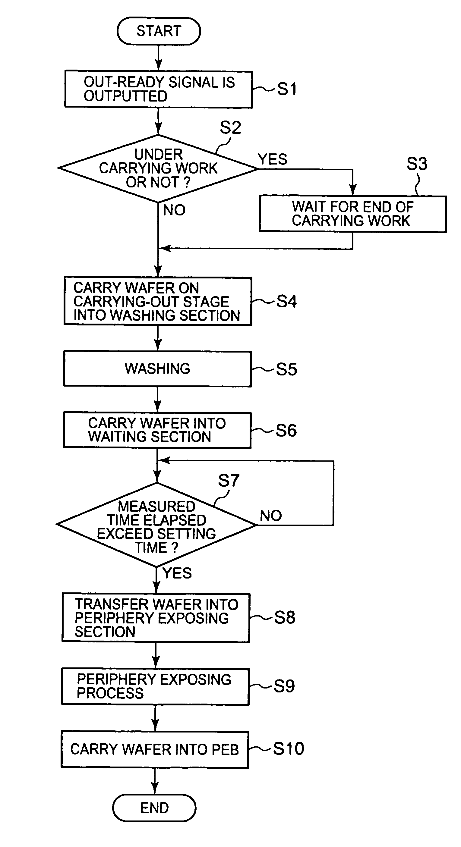
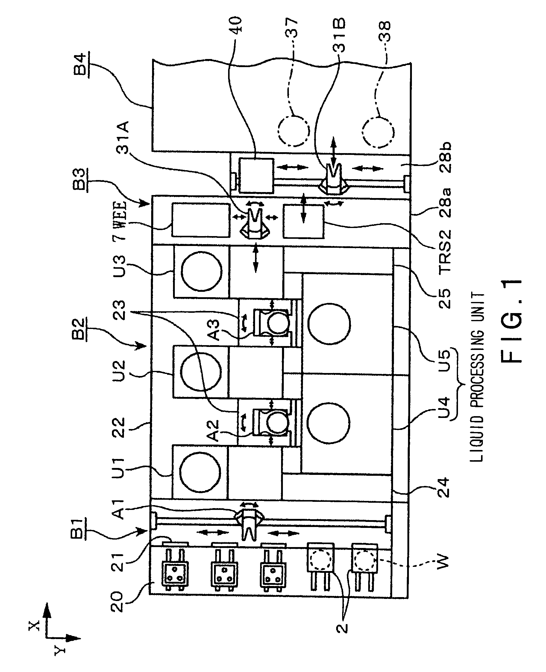
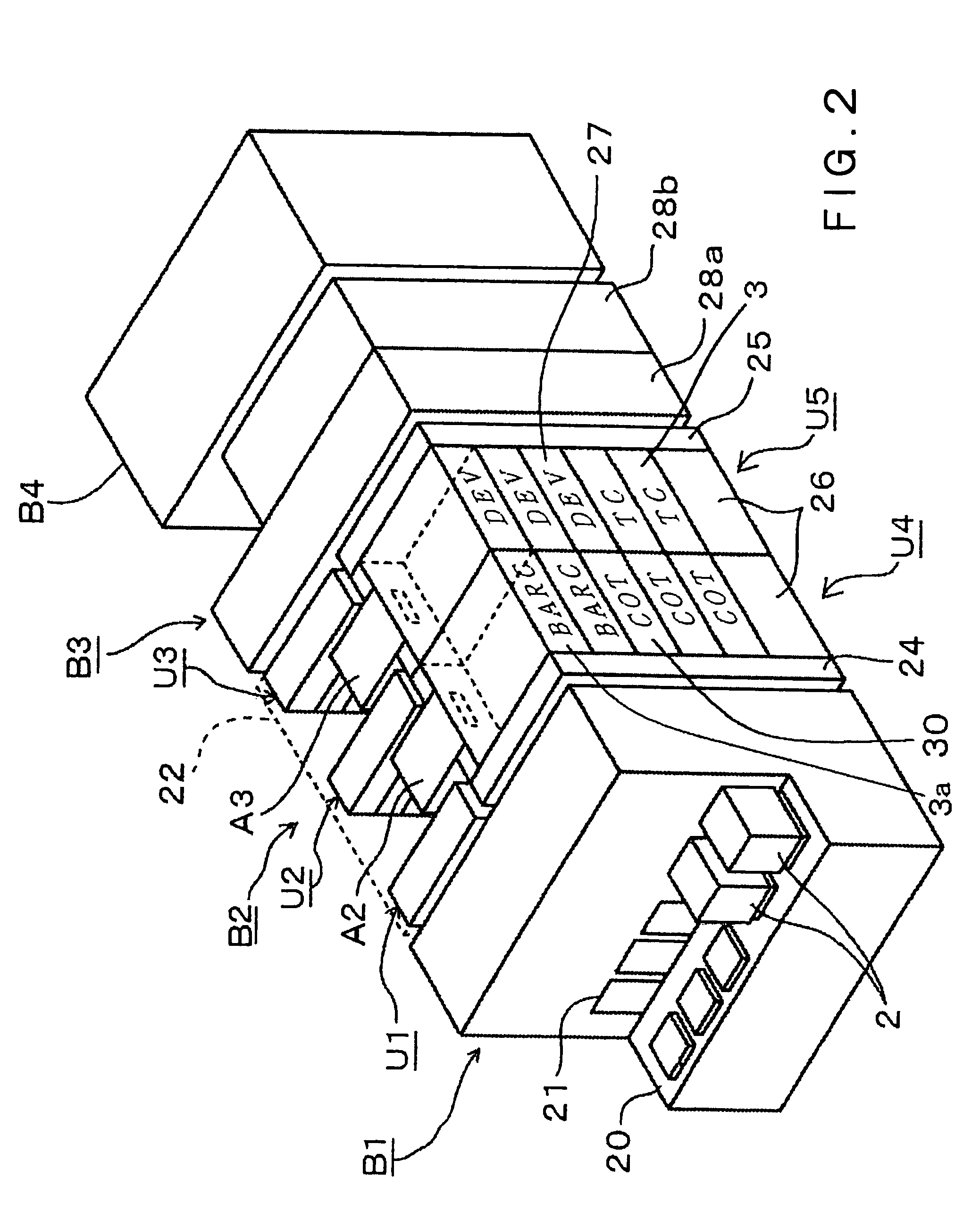
[0046]The whole construction of a system in which an exposing apparatus is connected with a coating and developing apparatus according to the present invention will be described briefly with reference to FIGS. 1 and 2. In FIGS. 1 and 2, reference character B1 designates a carrier station for carrying in and carrying out carriers 2, in which, for example, thirteen sheets of substrates are contained. The carrier station B1 includes a placing section 20 in which carriers 2 can be arranged in large numbers, opening and closing sections 21 each provided in a front wall when viewed from the placing section 20, and a transfer means A1 adapted to take out a wafer W from each carrier 2 via the corresponding opening and closing section 21.

[0047]On the back side of the carrier station B1, a processing block B2 which is surrounded by a housing 22 is provided. The processing block B2 includes rack units U1, U2, U3 successively arranged from the front side and each composed of heating and cooling...


PUM

PropertyMeasurementUnit
diameteraaaaaaaaaa
timeaaaaaaaaaa
sizeaaaaaaaaaa

Abstract

A coating and developing apparatus comprises a washing section for washing the surface of a substrate after it has been subjected to a dipping exposure process in an exposing apparatus, and a first substrate carrying means adapted to transfer the substrate carried out from the exposing apparatus after the dipping exposure process to the washing section. The first substrate carrying means is controlled by a control means. Namely, the control means controls the first substrate carrying means such that the substrate can be washed in the washing section in a period of time prior to a time zone in which the size of liquid drops remaining on the substrate due to the dipping exposure process becomes smaller quite rapidly, based on a carrying-out ready signal for the substrate from the exposing apparatus, by using a relationship between the time elapsed from the end of the dipping exposure process and the size of liquid drops remaining on the substrate due to the dipping exposure process.

Description

BACKGROUND OF THE INVENTION[0001]1. Field of the Invention[0002]The present invention is a coating and developing apparatus, and a coating and developing method for coating a resist liquid on a surface of a substrate and developing the substrate after a dipping exposure process.[0003]2. Background Art[0004]A method for forming a resist pattern on a substrate, such as a glass substrate for use in a semiconductor wafer (hereinafter referred to as a “wafers”) or LCD (Liquid Crystal Display) is carried out in a system composed by connecting a coating and developing apparatus comprising a coating section for coating a resist liquid on a substrate and a developing section for developing the substrate after exposure with an exposing apparatus.[0005]In an exposing technique of an exposing apparatus, in order to enhance resolution by improving the exposing technique employing an existing light source, for example, argon fluoride (ArF) or krypton fluoride (KrF), there is a method of exposing ...

Claims


Application Information

Patent Timeline
Patent Type & Authority Patents(United States)
IPC IPC(8): G06F19/00H01L21/469H01L21/31H01L21/20H05K3/00H01C17/06C23C26/00B28B19/00B29B15/10C23C18/00B05C9/12B05C9/14B05C13/02G03F7/30H01L21/027
CPCG03F7/2041H01L21/6715H01L21/67225H01L21/67276B05C11/10G03F7/70341
Inventor ISHIDA, SEIKIYAMAMOTO, TARO
Owner TOKYO ELECTRON LTD
Why Eureka
Try Eureka