Circuit with flexible portion

a flexible circuit and circuit board technology, applied in the field of electronic circuitry and modules, can solve the problems of generating significant amounts of heat for all components, complicated connections to the pcb in close proximity, and the characteristics of flexible circuitry, so as to and improve the flexibility of the flexible connector

Active Publication Date: 2010-10-12
NETLIST INC
View PDF134 Cites 94 Cited by
  • Summary
  • Abstract
  • Description
  • Claims
  • Application Information

AI Technical Summary

Benefits of technology

[0013]In certain embodiments, a circuit card comprises a rigid portion having a first plurality of contacts configured to be in electrical communication with a plurality of memory devices. The circuit card further comprises a flexible connector coupled to the rigid portion. The flexible connector has a first side and a second side. The flexible connector comprises a dielectric layer, a second plurality of contacts configured to be in electrical communication with a substrate, and a plurality of electrical conduits on the first side of the flexible connector and extending from the rigid portion to the second plurality of contacts. The plurality of electrical conduits is in electrical communication with one or more contacts of the first plurality of contacts and with the second plurality of contacts. The flexible connector further comprises an electrically conductive layer on the second side of the flexible connector. The electrically conductive layer is superposed with the plurality of electrical conduits with the dielectric layer therebetween. The electrically conductive layer does not cover one or more portions of the second side of the flexible connector, thereby providing improved flexibility of the flexible connector.
[0014]In certain embodiments, a memory module comprises a main printed-circuit board (PCB) having a first side and a second side. The main PCB comprises a plurality of edge connectors configured to be in electrical communication with corresponding socket connectors of a computer system. The main PCB further comprises a first plurality of contacts in electrical communication with the plurality of edge connectors. The memory module further comprises a first daughter circuit card positioned on the first side of the main PCB and oriented generally parallel to the main PCB. The first daughter circuit card comprises a rigid portion and a plurality of memory devices mounted thereto. The first daughter circuit card further comprises a flexible connector and a second plurality of contacts thereon. The second plurality of contacts is in electrical communication with the first plurality of contacts. The flexible connector has a first side and a second side. The flexible connector comprises a dielectric layer and a plurality of electrical conduits on the first side of the flexible connector. The plurality of electrical conduits is in electrical communication with the plurality of memory devices and the second plurality of contacts. The flexible connector further comprises an electrically conductive layer on the second side of the flexible connector. The electrically conductive layer is superposed with the plurality of electrical conduits with the dielectric layer therebetween. The electrically conductive layer does not cover one or more portions of the second side of the flexible connector, thereby providing improved flexibility of the flexible connector.
[0015]In certain embodiments, a computer system comprises a memory module comprising a printed-circuit board (PCB) having a first side and a second side. The PCB comprises a plurality of edge connectors configured to be in electrical communication with corresponding socket connectors of a computer system. The PCB further comprises a first plurality of contacts in electrical communication with the plurality of edge connectors. The memory module further comprises a first daughter circuit card positioned on the first side of the PCB and oriented generally parallel to the PCB. The first daughter circuit card comprises a rigid portion and a plurality of memory devices mounted thereto. The first daughter circuit card further comprises a flexible connector and a second plurality of contacts thereon. The second plurality of contacts is in electrical communication with the first plurality of contacts. The flexible connector has a first side and a second side. The flexible connector comprises a dielectric layer and a plurality of electrical conduits on the first side of the flexible connector. The plurality of electrical conduits is in electrical communication with the plurality of memory devices and the second plurality of contacts. The flexible connector further comprises an electrically conductive layer on the second side of the flexible connector. The electrically conductive layer is superposed with the plurality of electrical conduits with the dielectric layer therebetween. The electrically conductive layer does not cover one or more portions of the second side of the flexible connector, thereby providing improved flexibility of the flexible connector.

Problems solved by technology

Such components mounted in close proximity to the PCB can require complicated connections to the PCB.
Stacked PCB configurations in the prior art have used flexible circuitry or flex circuits to provide electrical connections between the stacked PCBs, but these configurations have been limited by the characteristics of the flexible circuitry.
Stacking configurations can cause problems due to power dissipation in the components which are in close proximity.
Some or all of the components can generate significant amounts of heat, which can raise the temperature of the component itself or of the surrounding components of the module.
The raised temperature of these components can have harmful effects on the performance of the components, causing them to malfunction.
However, the narrow air gap between the stacked PCBs would allow very little cool air from the ventilation fan to cool the components on the inside surfaces to within the specified operating temperatures.
Because these sockets are often in proximity to one another (e.g., spaced with approximately 9 millimeters on either side of the socket), there is a limited amount of space between the sockets which thereby limits the dimensions of a memory module installed therein.

Method used


Image

  • Circuit with flexible portion
  • Circuit with flexible portion
  • Circuit with flexible portion

Examples


Embodiment Construction

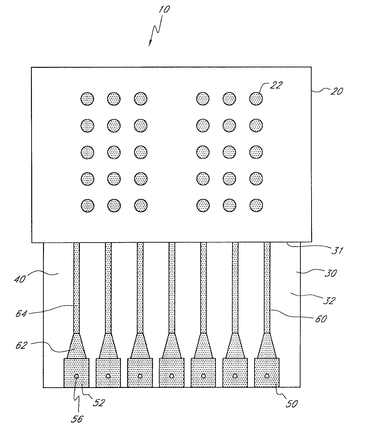
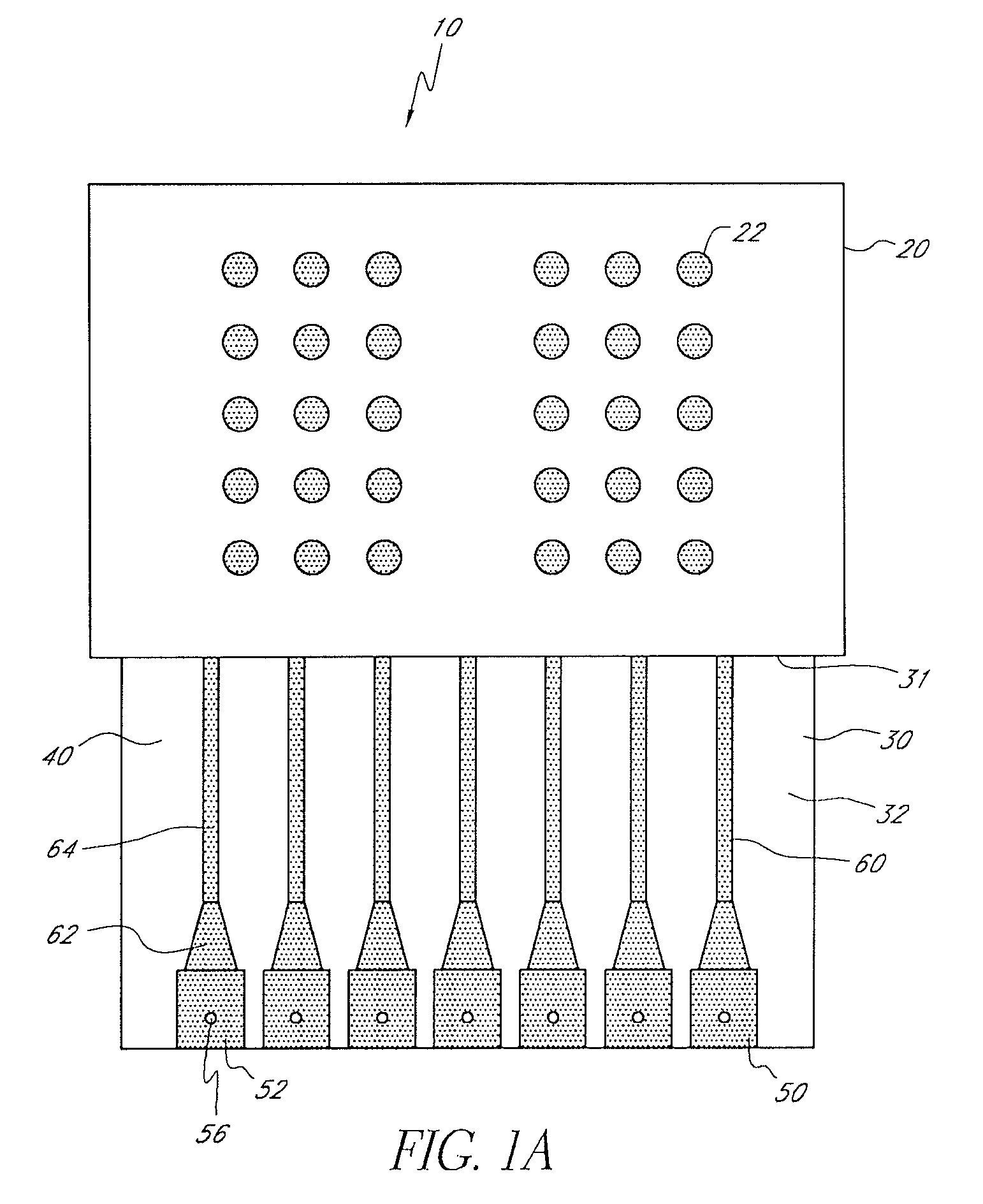
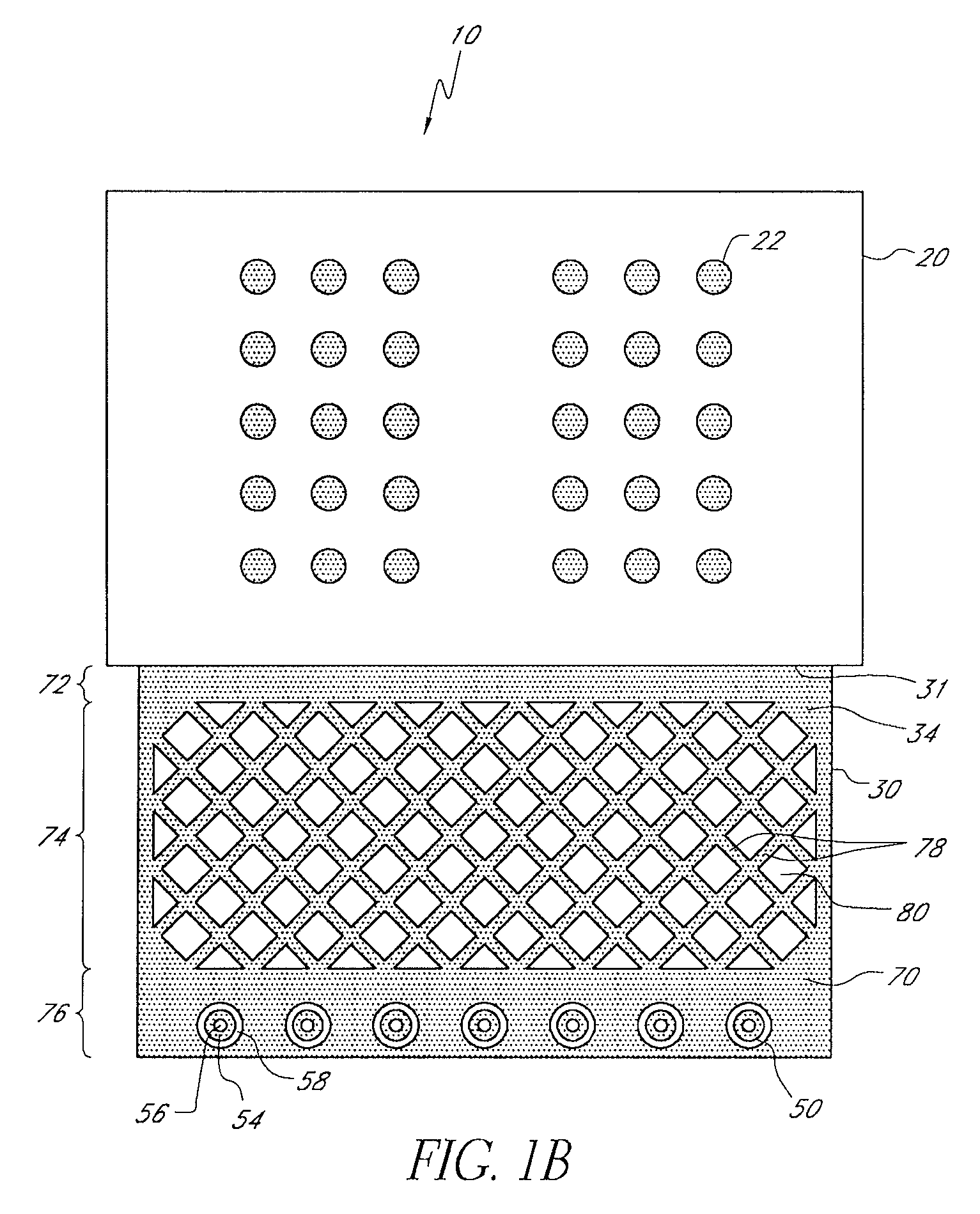
[0035]FIGS. 1A-1C schematically illustrate three views of an example circuit card 10 compatible with certain embodiments described herein. The circuit card 10 comprises a rigid portion 20 having a first plurality of contacts 22 configured to be in electrical communication with a plurality of memory devices (not shown). The circuit card 10 further comprises a flexible connector 30 coupled to the rigid portion 20. The flexible connector 30 has a first side 32 and a second side 34. The flexible connector 30 comprises a dielectric layer 40 and a second plurality of contacts 50 configured to be in electrical communication with a substrate (not shown). The flexible connector 30 further comprises a plurality of electrical conduits 60 on the first side 32 of the flexible connector 30 and extending from the rigid portion 20 to the second plurality of contacts 50. The plurality of electrical conduits 60 are in electrical communication with one or more contacts 22 of the first plurality of con...


PUM


Abstract

A circuit includes a first plurality of contacts configured to be in electrical communication with a plurality of electronic devices. The circuit card further includes a flexible portion including a dielectric layer, a second plurality of contacts, and a plurality of electrical conduits extending across a region of the flexible portion and in electrical communication with one or more contacts of the first plurality of contacts and with the second plurality of contacts. The flexible portion further includes an electrically conductive layer extending across the region of the flexible portion. The electrically conductive layer is superposed with the plurality of electrical conduits with the dielectric layer therebetween. The electrically conductive layer does not overlay one or more portions of the dielectric layer in the region of the flexible portion.

Description

RELATED APPLICATIONS[0001]This application is a continuation of U.S. patent application Ser. No. 11 / 511,523, filed Aug. 28, 2006, incorporated in its entirety by reference herein, which claims the benefit of priority from U.S. Provisional Patent No. 60 / 712,156, filed Aug. 29, 2005, which is incorporated in its entirety by reference herein.BACKGROUND OF THE INVENTION[0002]1. Field of the Invention[0003]This application relates generally to electronic circuitry and modules for computer-based applications, and more particularly to circuit cards, printed circuit boards, and memory modules.[0004]2. Description of the Related Art[0005]Computer systems often utilize modules comprising one or more circuit cards or printed circuit boards (PCBs). Each PCB has one or more components (e.g., integrated circuits or ICs) mounted thereon, and the components can be mounted on one side or on both sides of the PCB. In certain computer systems, the PCBs of the module are stacked next to one another to ...

Claims


Application Information

Patent Timeline
Patent Type & Authority Patents(United States)
IPC IPC(8): H01R12/00
CPCH05K1/147H01L2224/16225H05K1/0203H05K1/141H05K2203/1572H05K3/4691H05K2201/10159H05K2201/1056H01L2924/00011H01L2924/00014H01L2224/0401
Inventor BHAKTA, JAYESH R.YU, ENCHAOCHEN, CHI SHEFLAIG, RICHARD E.
Owner NETLIST INC
Why Eureka
Try Eureka