Fabrication of single or multiple gate field plates

a gate field and gate plate technology, applied in the field of single or multiple gate field plates, can solve the problems of low breakdown, low electric field, detrimental effects, etc., and achieve the effects of improving the performance of large periphery and/or sub-micron gate devices, tight control of dielectric material thickness, and reducing gate resistan

Active Publication Date: 2010-10-12
RGT UNIV OF CALIFORNIA +1
View PDF26 Cites 107 Cited by
  • Summary
  • Abstract
  • Description
  • Claims
  • Application Information

AI Technical Summary

Benefits of technology

[0011]Embodiments of the present invention provide improved methods of fabricating single and multiple gate field plates. A fabrication process according to the invention uses consecutive steps of dielectric material deposition or growth, dielectric material etch and metal evaporation on the surface of field effect transistors. The advantages of the fabrication process include tight control of the dielectric material thickness, and the absence of any exposure of the surface of the device active region to any dry or wet etch process that may induce damage in the semiconductor material forming the field effect transistor. Moreover, the dielectric material deposited on the device surface does not need to be removed from the device intrinsic regions, which enables the realization of field-plated devices without damage caused by the dry or wet etch processes. Using multiple gate field plates reduces gate resistance through the use of multiple connections, thus improving performances of large periphery and / or sub-micron gate devices. Finally, by properly adjusting the thickness of the dielectric material, parallel gate contacts can be deposited on top of the dielectric material, in order to significantly reduce gate resistance by electrically connecting the parallel gate contacts on device extrinsic regions.

Problems solved by technology

This results in a lower electric field in the device active region for a given bias voltage, alleviating all the detrimental effects (low breakdown, trapping phenomena, poor reliability) that take place whenever a device is operated at a high electric field.
Moreover, a field plate positioned in the gate drain access region has also the capability of modulating the device active region, resulting in a decrease of surface traps effects that prevent proper device operation under large radio frequency (RF) signals

Method used


Image

  • Fabrication of single or multiple gate field plates
  • Fabrication of single or multiple gate field plates
  • Fabrication of single or multiple gate field plates

Examples


Embodiment Construction

[0023]In the following description of the preferred embodiment, reference is made to the accompanying drawings which form a part hereof, and in which is shown by way of illustration a specific embodiment in which the invention may be practiced. It is to be understood that other embodiments may be utilized and structural changes may be made without departing from the scope of the present invention.

[0024]Overview

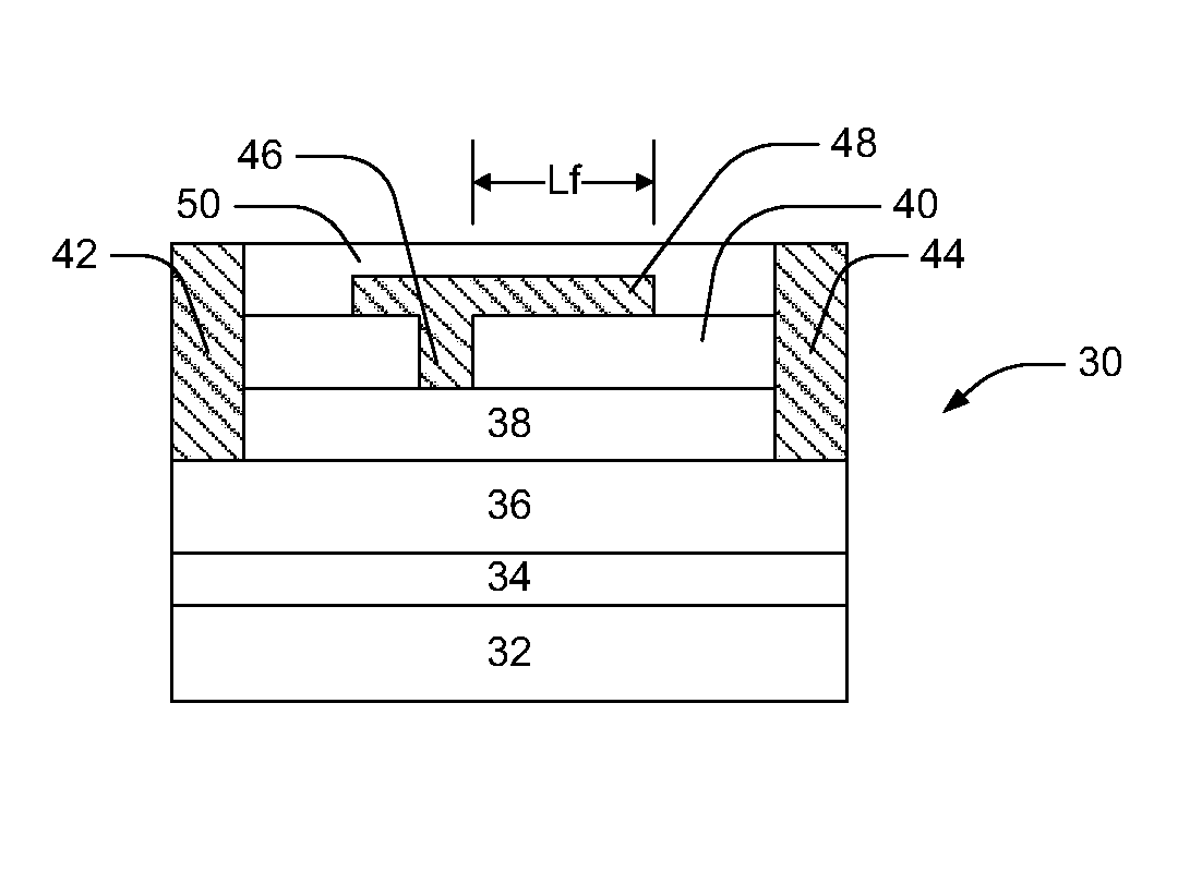
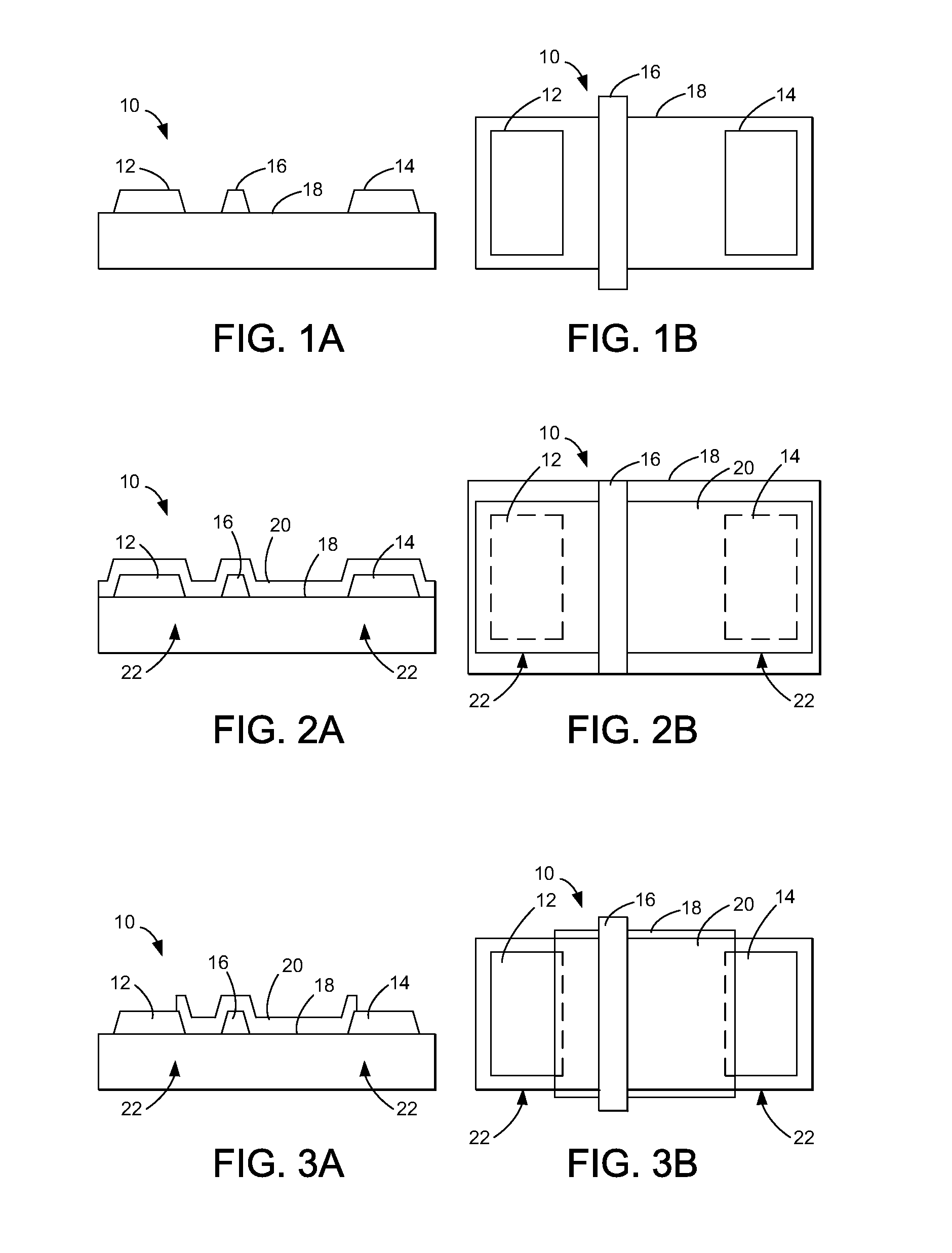
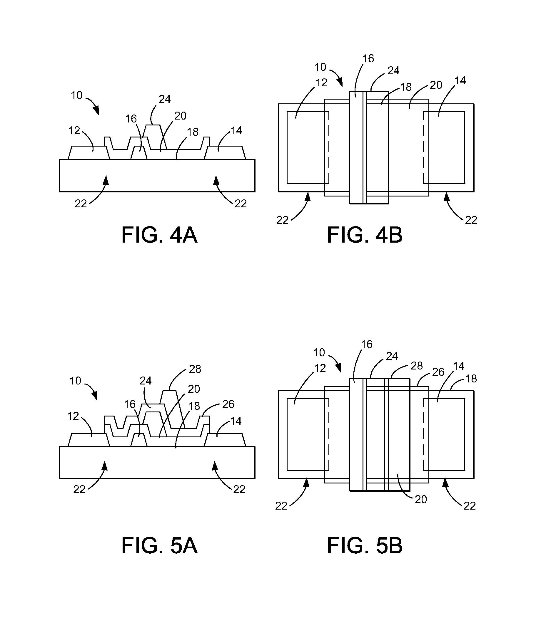
[0025]The present invention describes a simple fabrication process for the realization of single or multiple gate field plate structures for field effect transistors (FETs). The present invention uses simple and typically well-controlled consecutive processing steps of dielectric material deposition or growth, dielectric material etch and metal evaporation.

[0026]Fabrication Process

[0027]FIGS. 1A, 1B, 2A, 2B, 3A, 3C, 4A, and 4B illustrate the steps of one possible realization of the fabrication process according an embodiment of the invention, wherein the fabrication process co...


PUM


Abstract

A process for fabricating single or multiple gate field plates using consecutive steps of dielectric material deposition / growth, dielectric material etch and metal evaporation on the surface of a field effect transistors. This fabrication process permits a tight control on the field plate operation since dielectric material deposition / growth is typically a well controllable process. Moreover, the dielectric material deposited on the device surface does not need to be removed from the device intrinsic regions: this essentially enables the realization of field-plated devices without the need of low-damage dielectric material dry / wet etches. Using multiple gate field plates also reduces gate resistance by multiple connections, thus improving performances of large periphery and / or sub-micron gate devices.

Description

CROSS-REFERENCE TO RELATED APPLICATIONS[0001]This application claims the benefit under 35 U.S.C. §119(e) of the following and commonly-assigned U.S. Provisional Patent Application:[0002]Ser. No. 60 / 501,557, entitled “FABRICATION OF SINGLE OR MULTIPLE GATE FIELD PLATES,” filed on Sep. 9, 2003, by Alessandro Chini, Umesh K. Mishra, Primit Parikh, and Yifeng Wu;which application is incorporated by reference herein.STATEMENT REGARDING FEDERALLY SPONSORED RESEARCH AND DEVELOPMENT[0003]This invention was made with Government support under Grant No. N00014-01-1-0764 awarded by the ONR MURI program and Grant No. F49620-99-1-0296 awarded by the AFOSR MURI program. The Government has certain rights in this invention.BACKGROUND OF THE INVENTION[0004]1. Field of the Invention[0005]This invention relates to semiconductor devices, and more particularly, to the fabrication of single or multiple gate field plates.[0006]2. Description of the Related Art[0007](Note: This application references to var...

Claims


Application Information

Patent Timeline
Patent Type & Authority Patents(United States)
IPC IPC(8): H01L29/778H01LH01L29/40
CPCH01L27/0605H01L29/402H01L29/404H01L29/42312H01L29/66462H01L29/7787H01L29/2003H01L29/207H01L29/785H01L29/42316H01L29/41766H01L29/40117H01L21/18H01L29/768H01L29/205
Inventor CHINI, ALESSANDROMISHRA, UMESH K.PARIKH, PRIMITWU, YIFENG
Owner RGT UNIV OF CALIFORNIA
Why Eureka
Try Eureka