Wafer aligning apparatus and related method

a technology of wafer alignment and aligning apparatus, which is applied in the direction of instruments, television systems, image enhancement, etc., can solve the problems of reducing the productivity of a unit process apparatus, increasing the transfer time of wafers, and affecting the quality of wafers, so as to reduce the process execution time, promote the mounting of the wafer aligning apparatus, and reduce the effect of structural differences

Inactive Publication Date: 2010-10-12
SAMSUNG ELECTRONICS CO LTD
View PDF13 Cites 6 Cited by
  • Summary
  • Abstract
  • Description
  • Claims
  • Application Information

AI Technical Summary

Benefits of technology

[0011]Embodiments of the invention provide a wafer aligning apparatus and a related wafer aligning method, wherein the wafer aligning apparatus is adapted to align the center of the wafer as the wafer is loaded into a process chamber when certain conditions are met. In addition, embodiments of the invention provide a wafer aligning apparatus and a wafer aligning method capable of reducing process execution time by, when certain conditions are met, aligning the center of a wafer withdrawn from a load lock chamber while the wafer is being transferred to a process chamber without providing the wafer to an aligning chamber. Additionally, embodiments of the invention provide a wafer aligning apparatus having relatively few structural differences relative to a conventional unit process apparatus to promote mounting of the wafer aligning apparatus.

Problems solved by technology

Thus, the wafers stacked in the cassette may be moved minutely and misaligned when the cassette is moved or when it is placed in a load lock chamber.
However, a relatively small amount of time is spent performing a unit process on a wafer in a unit process apparatus, while a relatively large amount of time is spent supplying the wafer to a process chamber.
This difference is a principal factor that reduces the productivity of a unit process apparatus.
In particular, in a unit process apparatus, each wafer that is transferred from a load lock chamber to a process chamber must pass through an aligning chamber before it is provided to the process chamber, which increases wafer transfer time and thereby reduces the productivity of the unit process apparatus.

Method used


Image

  • Wafer aligning apparatus and related method
  • Wafer aligning apparatus and related method
  • Wafer aligning apparatus and related method

Examples


Embodiment Construction

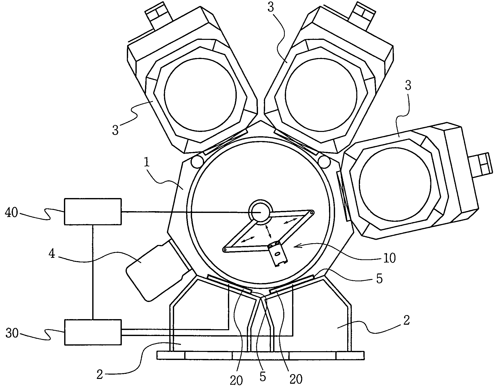
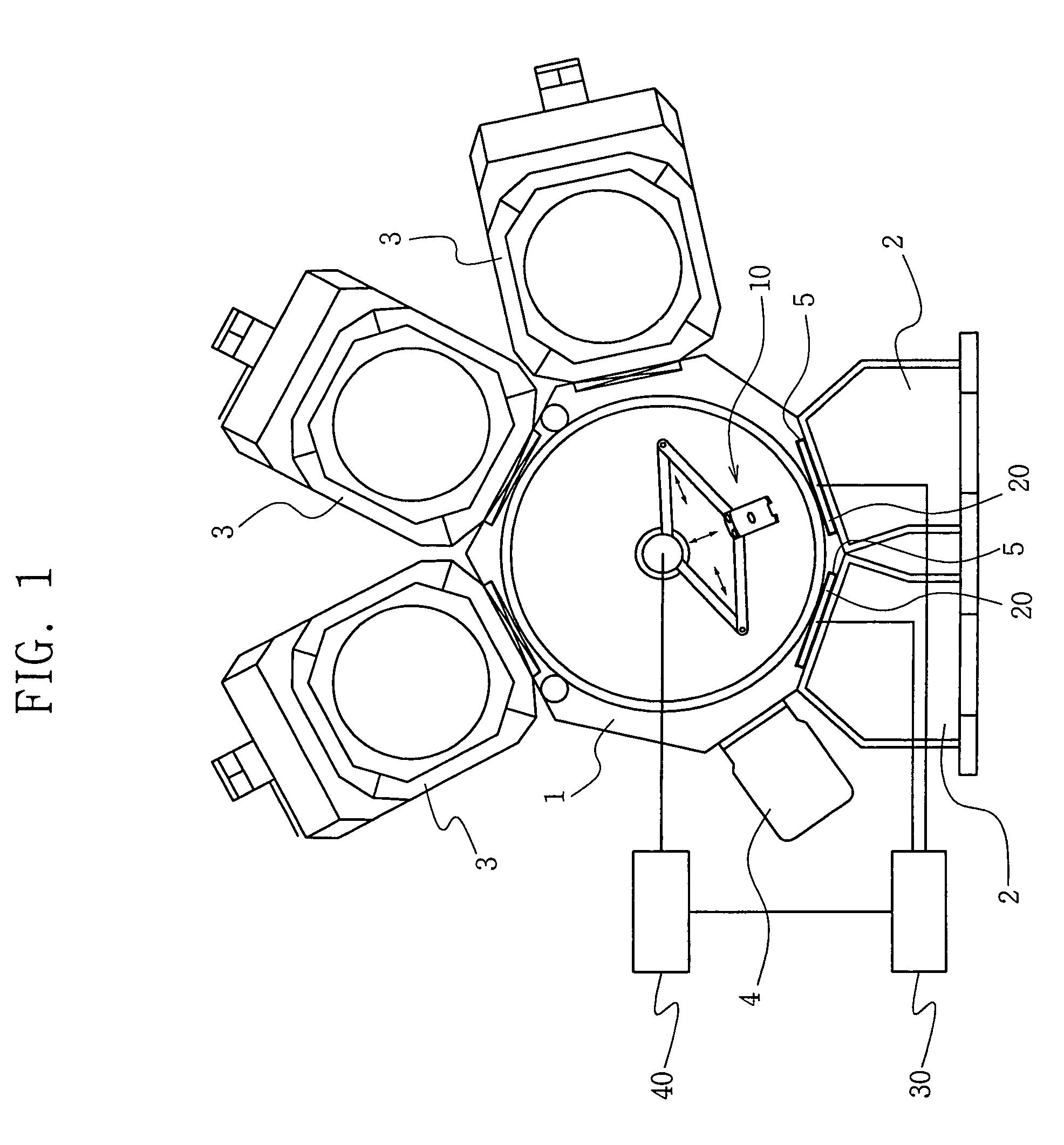
[0023]FIG. 1 is a plan view of a unit process apparatus comprising a wafer aligning apparatus in accordance with an embodiment of the invention.

[0024]In the embodiment illustrated in FIG. 1, a transfer chamber 1 comprises a transfer robot 10, load lock chambers 2 are disposed on a first side of transfer chamber 1, and process chambers 3, which perform substantive processes (i.e., unit processes), are disposed on a second side of transfer chamber 1 opposite load lock chambers 2. In addition, an aligning chamber 4 that may used to align a wafer before it is loaded into a process chamber 3 is disposed between one of the load lock chambers 2 and one of the process chambers 3 around the outside of transfer chamber 1. Though multiple load lock chambers 2 and process chambers 3 are shown in FIG. 1, for convenience of description, only one of the load lock chambers 2 (i.e., “load lock chamber 2”) and only one of the process chambers 3 (i.e., “process chamber 3”) will generally be referred t...


PUM


Abstract

Embodiments of the invention provide a wafer aligning apparatus and a wafer aligning method. In one embodiment, the wafer aligning apparatus comprises an imaging unit adapted to take an image of a wafer being transferred from a load lock chamber to a transfer chamber and adapted to convert the image into digital signals, and a signal processing unit adapted to calculate a center alignment correction value for the wafer by comparing the digital signals to a master image stored in the signal processing unit. The wafer aligning apparatus further comprises a robot controller adapted to receive the center alignment correction value from the signal processing unit and adapted to control a transfer robot in accordance with the center alignment correction value to provide the wafer to a process chamber such that the center of the wafer is substantially aligned.

Description

BACKGROUND OF THE INVENTION[0001]1. Technical Field[0002]Embodiments of the invention relate to a wafer aligning apparatus. In particular, embodiments of the invention relate to a wafer aligning apparatus adapted to load a wafer into a process chamber such that the center of the wafer is aligned and a related method.[0003]This application claims priority to Korean Patent Application No. 10-2006-0013557, filed Feb. 13, 2006, the subject matter of which is hereby incorporated by reference in its entirety.[0004]2. Description of Related Art[0005]In general, semiconductor devices are fabricated by sequentially performing a series of unit processes, such as photolithography, vapor deposition, etching, diffusion, metal wiring, and ion implantation. A unit process apparatus adapted to perform a unit process on wafers comprises a process chamber that performs the unit process of that unit process apparatus on a wafer, and a load lock chamber that temporarily stores the wafer before it is lo...

Claims


Application Information

Patent Timeline
Patent Type & Authority Patents(United States)
IPC IPC(8): G06K9/00G06K9/68H04N7/18
CPCG06T7/0028G06T7/0044H01L21/681G06T2207/30148G06T7/33G06T7/74Y10S414/136H01H23/025H01H23/04H01H23/14H01H23/205H01H23/24
Inventor LEE, HEOK-JAEKIM, SANG-HOPARK, HYU-RIMBAE, DO-INSEO, KEE-WEONEWOO, CHANG-WOO
Owner SAMSUNG ELECTRONICS CO LTD
Why Eureka
Try Eureka