Driving method of in-plane-switching mode LCD
a technology of in-plane switching and driving method, which is applied in the direction of static indicating devices, non-linear optics, instruments, etc., can solve the problems of not displaying images at a sufficiently high brightness level, and it is difficult for related art lcd panels to effectively display moving pictures
- Summary
- Abstract
- Description
- Claims
- Application Information
AI Technical Summary
Benefits of technology
Problems solved by technology
Method used
Image

Examples
first embodiment
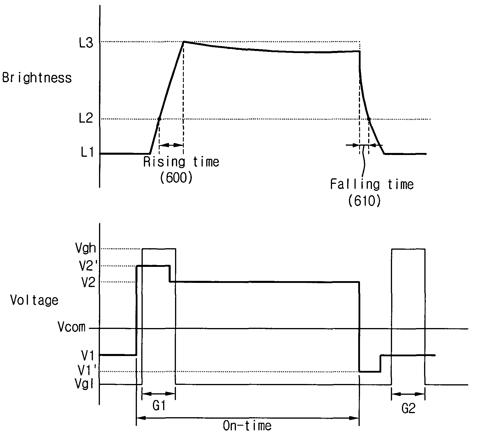
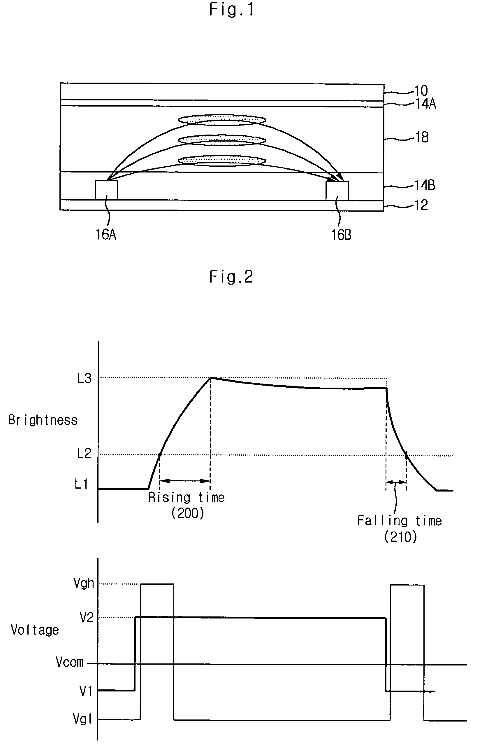
[0058]FIG. 6 illustrates waveforms of voltages applied to an IPS mode LCD panel in a driving method according to the present invention.
[0059]Referring to FIG. 6, TFTs within the LCD panel described above with respect to FIGS. 3-5 may be turned on or off in accordance with applied gate voltage. Therefore, when a gate high voltage Vgh of 21V is applied to a gate of a TFT, the gate is opened and the TFT is turned on. Conversely, when a gate low voltage Vgl of −5V is applied to a gate of a TFT, the gate is closed and the TFT is turned off. Further, the common voltage Vcom applied to the common electrode may constitute a uniform DC waveform. Moreover, data signal voltages V2 and V1 may be alternately applied to the pixel electrode of the LC cell in accordance with a driving frequency of the LCD panel. In one aspect of the present invention, the polarity of data signal voltage V2 may be opposite the polarity of data signal voltage V1.
[0060]According to principles of the present invention,...
second embodiment
[0063]FIG. 7 illustrates waveforms of voltages applied to an IPS mode LCD panel in a driving method according to the present invention.
[0064]The waveforms exemplarily illustrated in FIG. 7 may be essentially identical to those illustrated in FIG. 6. However, as shown in FIG. 7, a compensation voltage Vcom′, having the same polarity as the data signal voltage V2, instead of the compensation voltage V1′, may be applied to the common electrode, instead of the data line, for a predetermined amount of time before a second gate-ON period G2. In one aspect of the present invention, the compensation voltage Vcom′ may be applied to the common electrode before the data signal voltage V1 is applied to the data line in accordance with the driving frequency of the LCD panel.
[0065]While the second embodiment does not under drive the LC cell as described above with respect to the first embodiment, the second embodiment effects a reduction in falling time 710 of the LC cell as in the preceding embo...
third embodiment
[0067]FIG. 8 illustrates waveforms of voltages applied to an IPS mode LCD panel in a driving method according to the present invention.
[0068]As shown in FIG. 8, the principles of the present invention, outlined above with respect to FIG. 6, may be applied to reduce the response time required to display any gray level.
[0069]For example, the response time required to increase the gray level of an image exhibited by an LC cell from L4 to L5 may be reduced by applying a compensation voltage V5′ having a value greater than a data signal voltage V5, corresponding to the gray level L5. Subsequent to the over-driving, the data signal voltage V5 may be applied to the data line for a predetermined amount of time.
[0070]Further, the response speed required to reduce the gray level of an image exhibited by the LC cell from L5 to L6 may be reduced by applying a compensation voltage V6′ having a value less than a data signal voltage V6, corresponding to gray level L6. Subsequent to the under-drivi...
PUM
| Property | Measurement | Unit |
|---|---|---|
| voltage Vgh | aaaaa | aaaaa |
| voltage Vgl | aaaaa | aaaaa |
| voltage | aaaaa | aaaaa |
Abstract
Description
Claims
Application Information
 - R&D
- Intellectual Property
- Life Sciences
- Materials
- Tech Scout
- Unparalleled Data Quality
- Higher Quality Content
- 60% Fewer Hallucinations
Browse by: Latest US Patents, China's latest patents, Technical Efficacy Thesaurus, Application Domain, Technology Topic, Popular Technical Reports.
© 2025 PatSnap. All rights reserved.Legal|Privacy policy|Modern Slavery Act Transparency Statement|Sitemap|About US| Contact US: help@patsnap.com