Method for manufacturing integrated circuit

a manufacturing method and technology for integrated circuits, applied in the manufacture of printed circuits, transistors, solid-state devices, etc., can solve the problems of difficult handling of integrated circuits formed by thin films according to the present invention, and achieve the effects of improving mass productivity, high flexibility, and hardly broken

Inactive Publication Date: 2010-10-26
SEMICON ENERGY LAB CO LTD
View PDF37 Cites 27 Cited by
  • Summary
  • Abstract
  • Description
  • Claims
  • Application Information

AI Technical Summary

Benefits of technology

[0007]According to the present invention, the present invention has a means of making the thin film integrated circuit be fixated (a means for fixating a thin film integrated circuit). According to the present invention, a region that is not provided with the release layer is provided as a specific means for fixating a thin film integrated circuit (That is, the release layer is partially provided for fixating a thin film integrated circuit.). As a result, the thin film integrated circuit is integrated with the substrate, and so the thin film integrated circuit does not fly when the thin film integrated circuit moves or the pressure in a reaction chamber is controlled. Thereafter, the thin film integrated circuit is transposed to the supporting substratum having an adhesion surface, and the thin film integrated circuit is transposed to another substratum. In this instance, the adhesion strength of the supporting substratum is lower than that of another substratum. As a result, the thin film integrated circuit can be transposed to another substratum at once, and so mass productivity can be improved. During the process, the thin film integrated circuit does not fly in all directions since it is fixated.
[0008]According to the present invention, a means for pressing the integrated circuit is used as another means for fixating a thin film integrated circuit. As the means for pressing, a supporting substratum having an adhesion surface can be used. For instance, a substrate having an adhesion force such as silicon rubber can be used. Then, the release layer is removed in the state that the thin film integrated circuit is pressed by the means for pressing. As a result, the thin film integrated circuit does not fly when the thin film integrated circuit moves or the pressure in a reaction chamber is controlled since it can remain the state of being integrated with the substrate. Thereafter, the thin film integrated circuit is transposed. In this instance, the adhesion strength of the supporting substratum is lower than that of another substratum. That is, the thin film integrated circuit is transposed to another substratum having higher adhesion strength than that of the supporting substratum. As a result, the thin film integrated circuit can be transposed to another substratum at once, and so mass productivity can be improved. During the process, the thin film integrated circuit does not fly since it is fixated.
[0010]According to the present invention, a multiple thin film integrated circuits can be transposed to another substratum at once without flying the thin film integrated circuits when the thin film integrated circuit moves or the pressure in a reaction chamber is controlled. As a result, mass productivity can be improved.
[0011]Since the IDF chip according to the present invention is extremely thinner than that of an IC chip formed by a silicon wafer, the IDF chip does not detract from the design of a good when it is mounted to the good. Such the thin and lightweight IDF chip having a high flexible property is hardly broken, which is different from the IC chip formed by a silicon wafer.
[0012]Since the IDF chip according to the present invention is formed over an insulating substrate, there is no limitation on a mother substrate shape, which is also different from the IC chip formed by a silicon wafer. Therefore, mass productivity can be improved and the IDF chip can be mass-produced. As a result, the cost of the IDF chip can be expected to be reduced. The unit price of the IDF chip is so low. Accordingly, reducing the unit price of the IDF chip can yield an extremely large profit.

Problems solved by technology

The handling of the integrated circuit formed by the thin film according to the present invention has been difficult since there is fear that the integrated circuit is filed during moving due to its extreme light weight.

Method used


Image

  • Method for manufacturing integrated circuit
  • Method for manufacturing integrated circuit
  • Method for manufacturing integrated circuit

Examples


embodiment 1

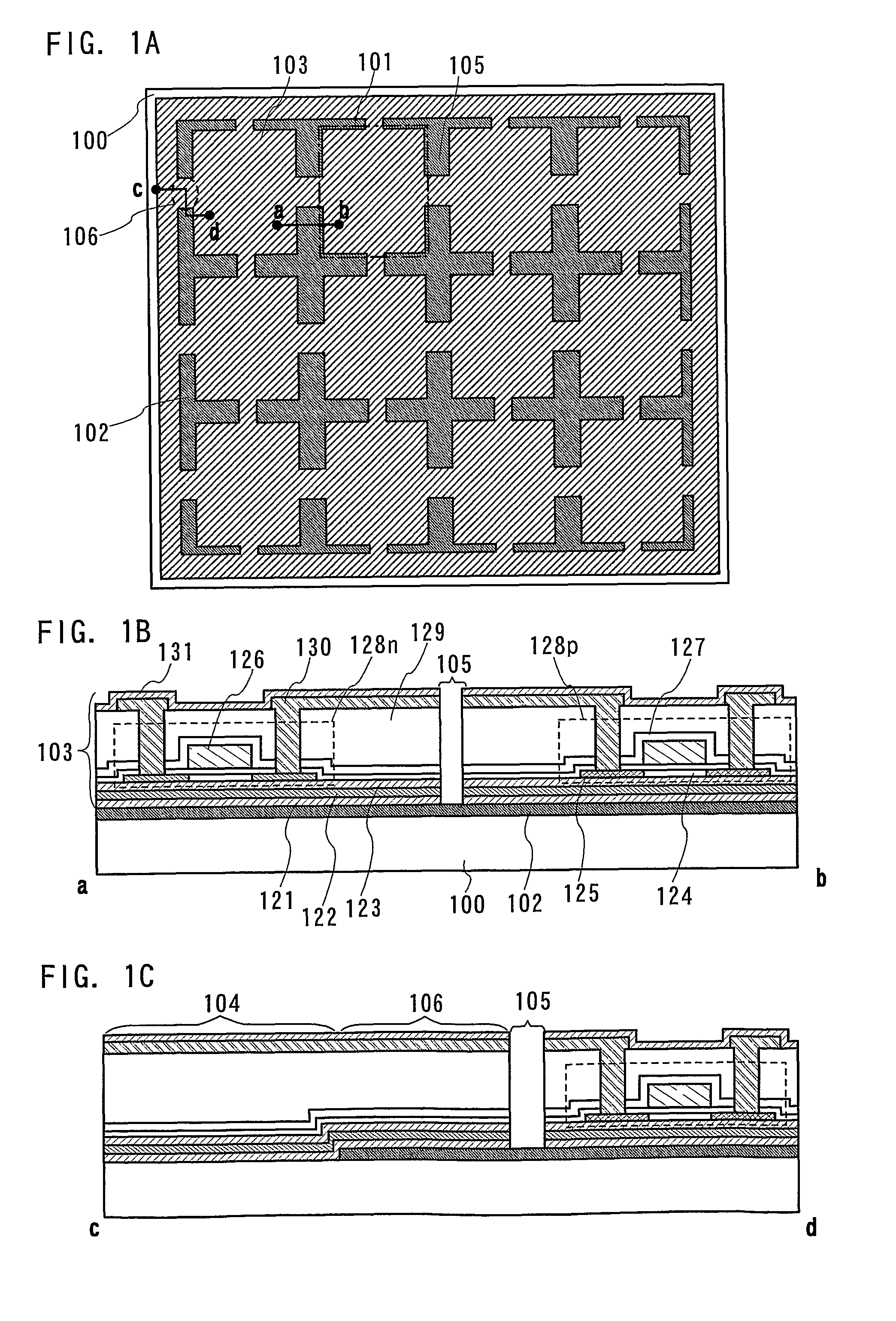
[0037]In this embodiment, a method for manufacturing a thin film integrated circuit provided with a region that does not form a release layer as a means for fixating the thin film integrated circuit is explained.

[0038]As illustrated in FIG. 1A, a release layer 102 and a layer 103 having a thin film transistor (also referred to as a TFT) that has a semiconductor film as an active region (hereinafter, TFT layer) are sequentially formed over an insulating substrate 100. A plurality of thin film integrated circuits 101 is formed. FIG. 1B illustrates a cross-sectional view of FIG. 1A taken along line a-b. FIG. 1C illustrates a cross-sectional view of FIG. 1A taken along line c-d.

[0039]As the insulating substrate 100, a glass substrate such as barium borosilicate glass or alumino-borosilicate glass, a quartz substrate, or the like can be used. As another insulating substrate, a substrate made from plastic as typified by poly ethylene terephthalate (PET), poly ethylene naphthalate (PEN), p...

embodiment 2

[0109]In this embodiment, an example of a manufacturing device of the thin film integrated circuit explained in Embodiment 1 is explained.

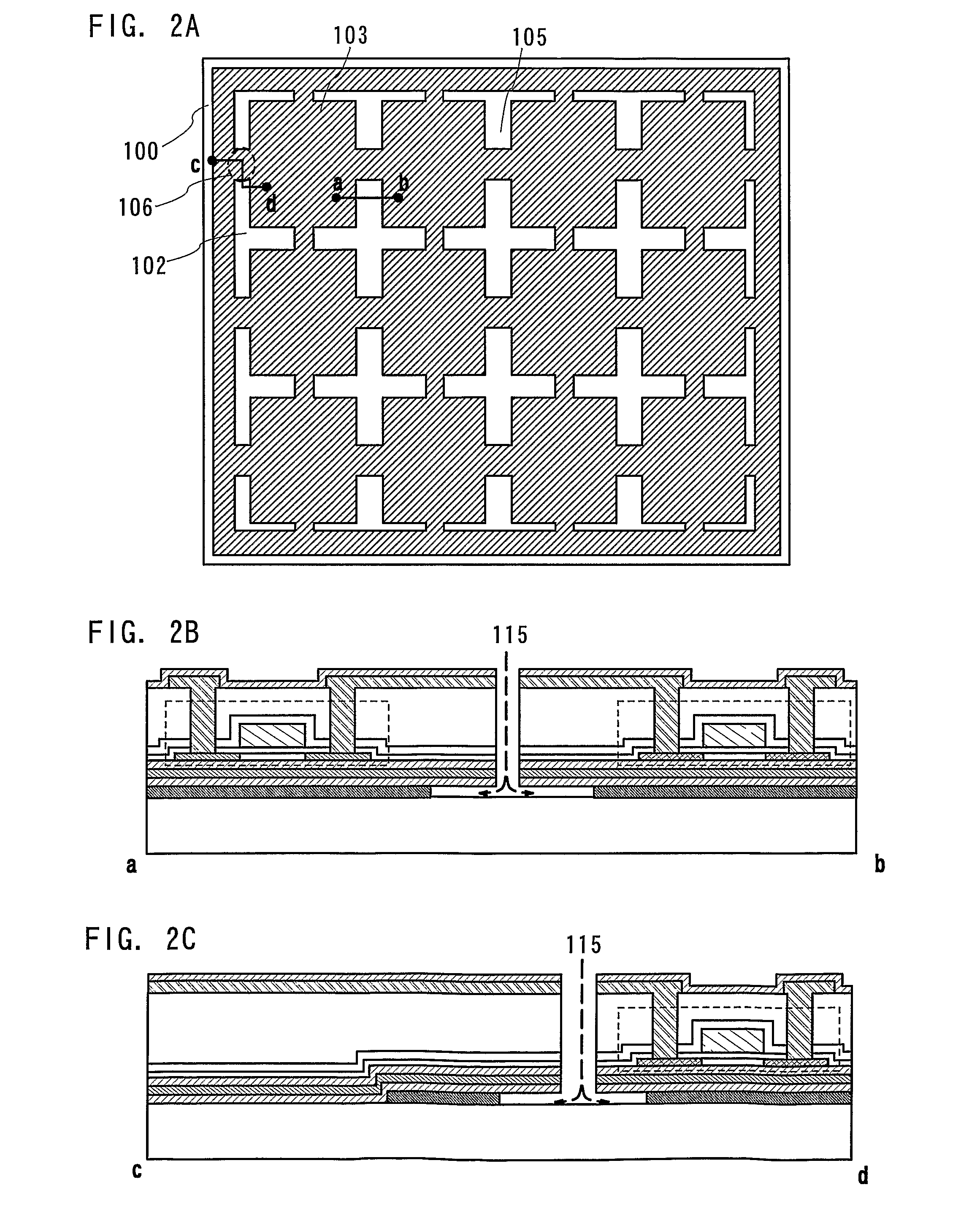
[0110]FIG. 6 illustrates a delivery carrier 201, a delivery elevator 202, a belt conveyor 203, a transportation roll 204, a film delivery roll 205, a discharge carrier 206, a discharge elevator 207, rollers 208a, 208b, 208c, and 208d, an operation evaluation device 209, a film delivery roll 210, an alignment device 211, and a take-up roll 212. A thing provided with an adhesion surface with respect to an upper surface of the thin film integrated circuit, that is, so-called tape, is delivered from the film delivery roll 205.

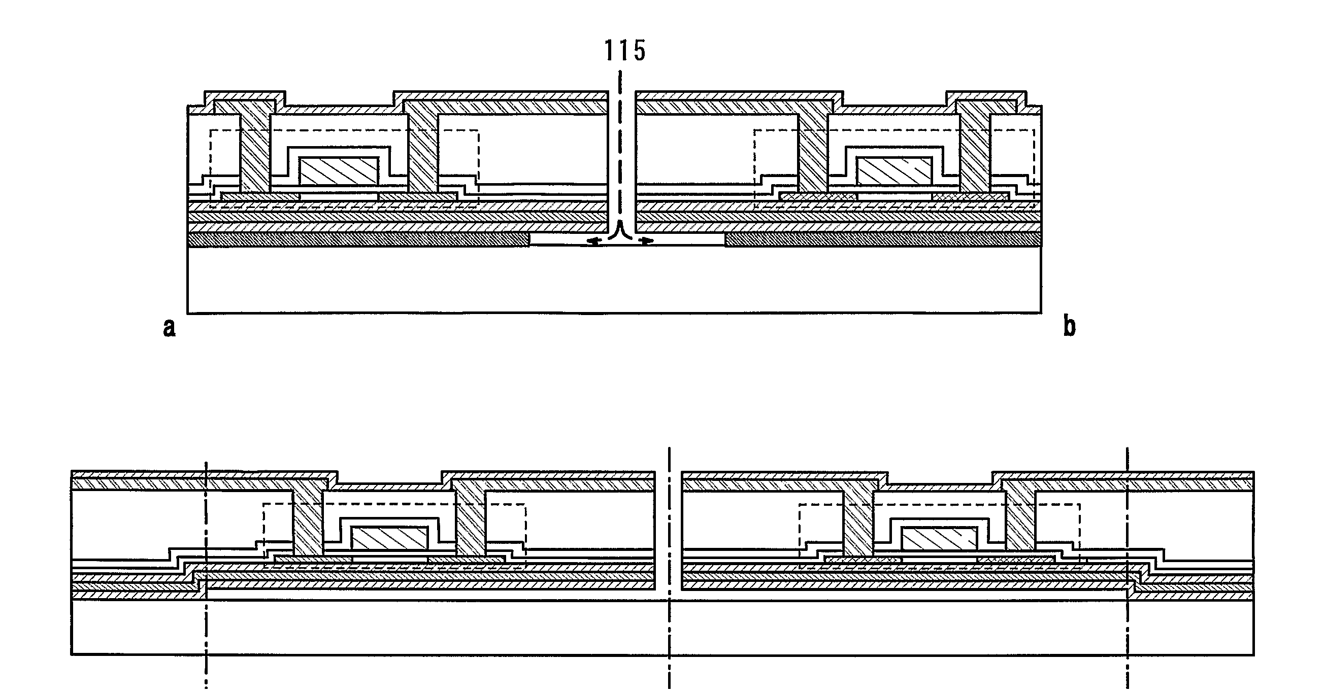
[0111]As illustrated in FIGS. 2A-C, a thin film integrated circuit in which a release layer 102 is removed is arranged over the belt conveyor 203 by transporting from the delivery carrier 201. Then, the thin film integrated circuit connected by a connection region 106 is transposed to the transportation roller 204 that correspond...

embodiment 3

[0121]In this embodiment, a method for manufacturing a thin film integrated circuit by using a means for pressing the thin film integrated circuit as a means for fixation is explained. Like structure such as the thin film integrated circuit as in Embodiment 1 is not further described in this embodiment, but another structure is explained.

[0122]As illustrated in FIG. 7A, a plurality of thin film integrated circuits 101 is formed by sequentially forming a release layer 102 and a TFT layer 103 having a semiconductor film as an active region over an insulating substrate 100 as is the case with Embodiment 1. FIG. 7B is a cross-sectional view of FIG. 7A takes along line of a-b, whereas FIG. 7C is a cross-sectional view of FIG. 7A taken along line of c-d.

[0123]Different from Embodiment 1, a region that is not provided with the release layer 102 may not be provided. That is, the release layer 102 is formed over the entire surface of the insulating substrate 100. Therefore, a connecting regi...


PUM


Abstract

A method for separating an integrated circuit formed by a thin film having a novel structure or a method for transferring the integrated circuit to another substrate, that is, so-called transposing method, has not been proposed. According to the present invention, in the case that an integrated circuit having a thin film having a novel structure formed over a substrate via a release layer is separated, the release layer is removed in the state that the thin film integrated circuit is fixated, the thin film integrated circuit is transposed to a supporting substrate having an adhesion surface, and the thin film integrated circuit is transposed to another substrate having an adhesion surface with higher strength of adhesion than that of the supporting substrate.

Description

TECHNICAL FIELD[0001]The present invention relates to a method for separating an integrated circuit or the like formed by a thin film and a method for manufacturing the integrated circuit.BACKGROUND ART[0002]A method for separating an integrated circuit using the conventional silicon wafer (hereinafter, IC chip) from a substrate has been proposed (Unexamined Patent Publication No. 2003-209073). The Unexamined Patent Publication No. 2003-209073 disclosed that a protective tape is adhered to a circuit surface of a semiconductor wafer, a dicing tape is adhered to a reverse surface, and the semiconductor wafer is diced with the protective tape to form a chip, then, a release tape is adhered to the diced protective tape, and then, the protective tape is heated to be deformed, lastly, the protective tape that is diced with the release tape is separated from the chip.[0003]As a method for mounting an optical device chip on an electronic circuit board, a method for making a crystal growth o...

Claims


Application Information

Patent Timeline
Patent Type & Authority Patents(United States)
IPC IPC(8): H01L21/00H01L21/02H01L21/336H01L21/762H01L21/77H01L21/84H01L27/12H01L29/786H05K3/20
CPCH01L27/1266H01L27/1214H01L21/76251H05K3/20H01L21/02H01L21/30
Inventor TSURUME, TAKUYAMARUYAMA, JUNYADOZEN, YOSHITAKA
Owner SEMICON ENERGY LAB CO LTD
Why Eureka
Try Eureka