LDMOS using a combination of enhanced dielectric stress layer and dummy gates

a dielectric stress layer and enhanced dielectric technology, applied in the manufacturing of semiconductor/solid-state devices, basic electric elements, electric apparatus, etc., can solve the problems of increasing complexity of technology, increasing the difficulty of maintaining carrier mobility in devices of the deep submicron generation, and new methods are needed

Active Publication Date: 2010-11-02
CHARTERED SEMICONDUCTOR MANUFACTURING
View PDF13 Cites 14 Cited by
  • Summary
  • Abstract
  • Description
  • Claims
  • Application Information

AI Technical Summary

Problems solved by technology

As devices are scaled down, however, the technology becomes more complex and new methods are needed to maintain the expected performance enhancement from one generation of devices to the next.
There is great difficulty in keeping carrier mobility high in devices of the deep submicron generations.

Method used


Image

  • LDMOS using a combination of enhanced dielectric stress layer and dummy gates
  • LDMOS using a combination of enhanced dielectric stress layer and dummy gates
  • LDMOS using a combination of enhanced dielectric stress layer and dummy gates

Examples


first example embodiment

I. First Example Embodiment

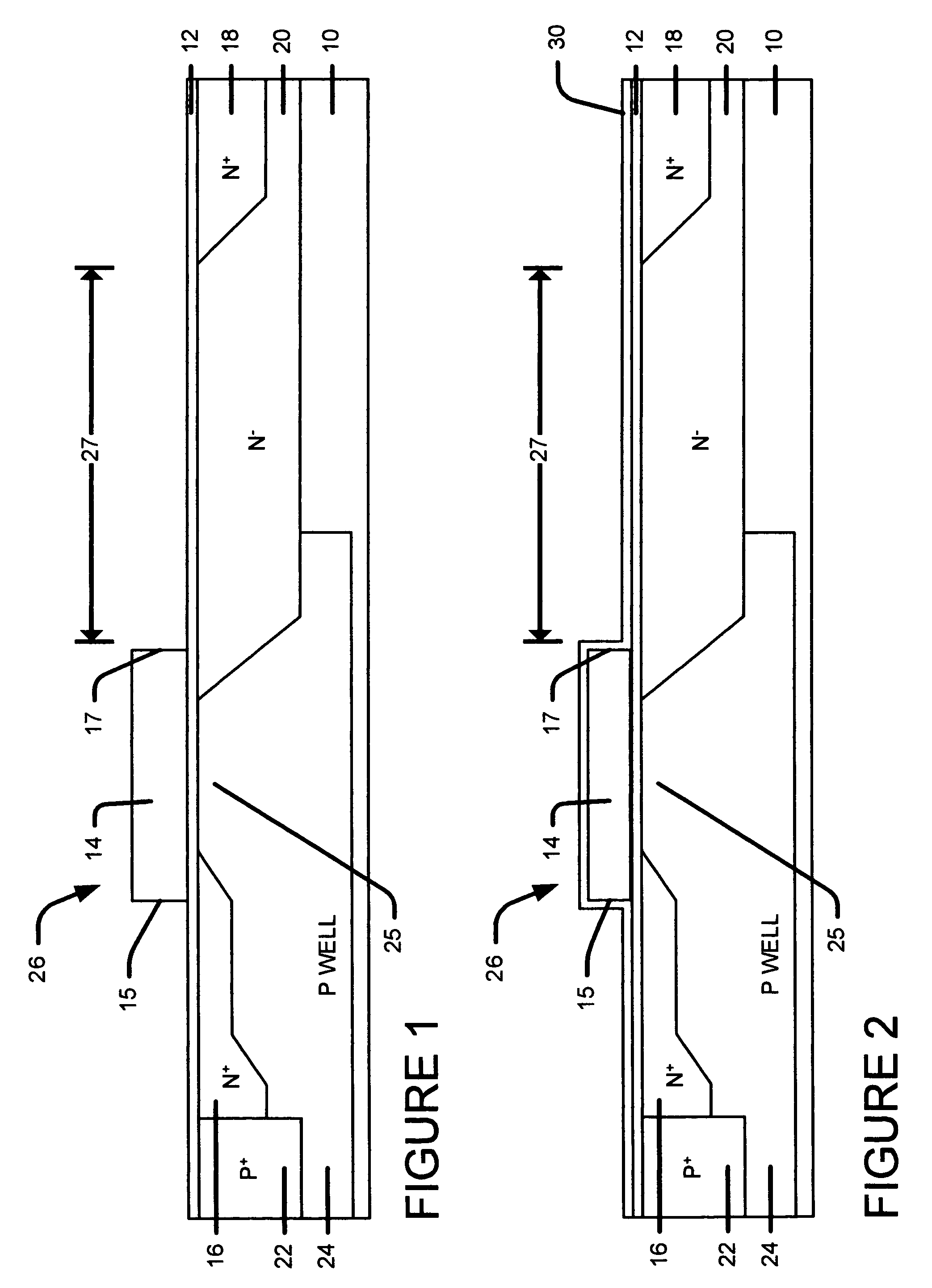
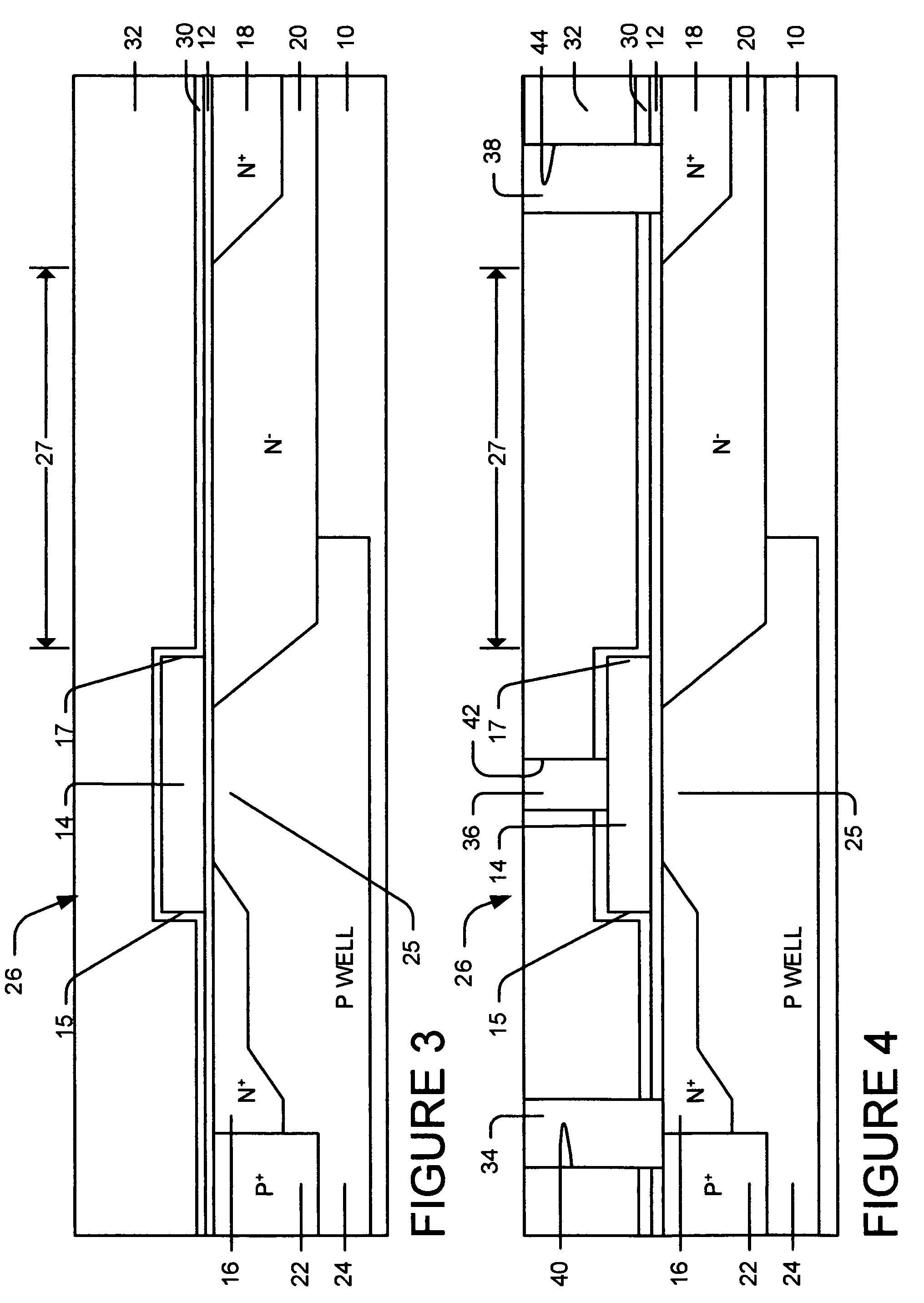
[0046]FIGS. 1 to 4 illustrate a first exemplary embodiment of the present invention wherein a stress layer is formed over the substrate and gate of an LDMOS. The stress layer that exerts stress into the channel under a (lateral double diffused metal-oxide-semiconductor) LDMOS gate. The resulting structure is illustrated in FIG. 4.

[0047]A N-type LDMOS (N LDMOS) is illustrated but the embodiment is not limited to n-type or LDMOS devices.

[0048]FIG. 1, in an exemplary embodiment of the present invention, an LDMOS 26 includes substrate 10 having dielectric layer 12 formed thereover to a thickness of, for example, from about 10 to 2000 angstroms. Substrate 10 may be comprised of, for example, silicon (Si), SiGe, or SiC and preferably silicon. The substrate can be a silicon on insulator (SOI) substrate.

[0049]Gate dielectric layer 12 may be comprised of, for example, silicon oxide, silicon oxynitride (SiON), HfO2 or ZrO2 and preferably silicon oxide.

[0050]Gate 14 ...

second example embodiment

II. Second Example Embodiment

Dummy Gates and Stress Layer

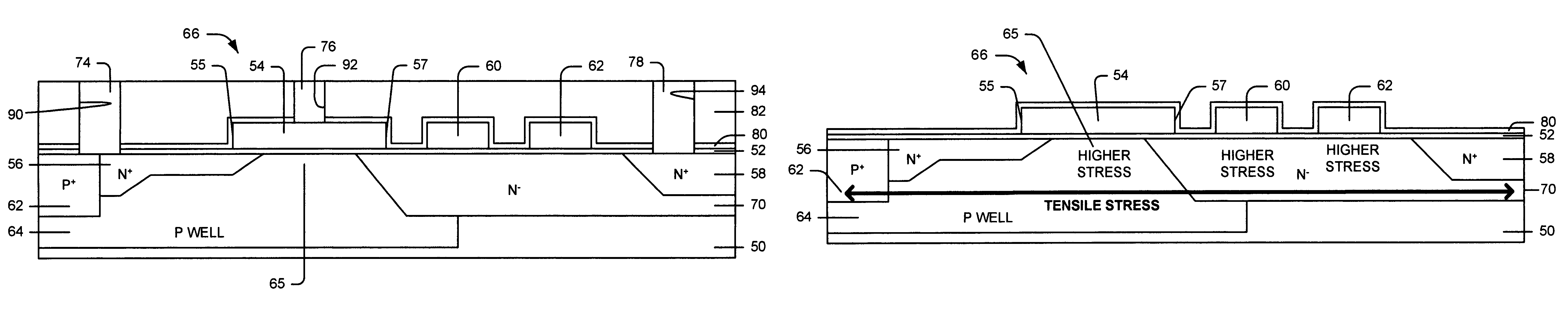
[0074]FIGS. 5 to 8 illustrate a second exemplary embodiment of the present invention wherein one or more dummy gate structures are also formed over the substrate at least within the second junction region (offset drain). A stress layer is formed over the dummy gates and substrate and gate and of the LDMOS. The stress layer has an inherent stress that exerts stress into the channel under a LDMOS gate. The resulting structure is illustrated in FIG. 8.

[0075]FIG. 5, in an exemplary embodiment of the present invention, an LDMOS 66 includes substrate 50 having gate dielectric layer 52 formed thereover to a thickness of, for example, from about 10 to 2000 angstroms. Substrate 50 may be comprised of, for example, silicon (Si), silicon germanium (SiGe) or silicon carbide (SiC) and preferably silicon.

[0076]Gate dielectric layer 52 may be comprised of, for example, silicon oxide, silicon oxynitride (SiON), HfO2 or ZrO2 and preferably sil...


PUM


Abstract

First example embodiments comprise forming a stress layer over a MOS transistor (such as a LDMOS Tx) comprised of a channel and first, second and third junction regions. The stress layer creates a stress in the channel and the second junction region of the Tx. Second example embodiments comprises forming a MOS FET and at least a dummy gate over a substrate. The MOS is comprised of a gate, channel, source, drain and offset drain. At least one dummy gate is over the offset drain. A stress layer is formed over the MOS and the dummy gate. The stress layer and the dummy gate improve the stress in the channel and offset drain region.

Description

BACKGROUND OF THE INVENTION[0001]1. Field of the Invention[0002]This invention relates generally to fabrication of semiconductor devices and more particularly to a lateral double diffused metal-oxide-semiconductor (LDMOS) and the fabrication of same.[0003]2. Description of the Prior Art[0004]Today's integrated circuits can include a huge number of transistors, capacitors, or other semiconductor devices formed in a semiconductor. Smaller devices are the key to enhance performance and to increase reliability in devices. As devices are scaled down, however, the technology becomes more complex and new methods are needed to maintain the expected performance enhancement from one generation of devices to the next. This relates mainly toward the primary semiconducting material of microelectronics, namely Silicon (Si), or more broadly, to Si based materials. One of the most important indicators of device performance is the carrier mobility. There is great difficulty in keeping carrier mobili...

Claims


Application Information

Patent Timeline
Patent Type & Authority Patents(United States)
IPC IPC(8): H01L21/332H01L21/336
CPCH01L29/66659H01L29/7835H01L29/7843H01L29/7846H01L29/404H01L29/456H01L29/49H01L29/4975H01L29/517H01L29/518
Inventor CHU, SANFORDLI, YISUOZHANG, GUOWEIVERMA, PURAKH RAJ
Owner CHARTERED SEMICONDUCTOR MANUFACTURING
Why Eureka
Try Eureka