

Display device
a display device and active matrix technology, applied in the field of display devices, can solve the problems of high manufacturing cost of a display device using the inability to simply employ the pixel circuit of a display device which is driven by the active matrix driving method using the organic el element, and the inability to meet the requirements of large-area or high-definition display devices. to achieve the effect of reducing voltage, improving reliability and yield, and manufacturing at low cos
- Summary
- Abstract
- Description
- Claims
- Application Information
AI Technical Summary
Benefits of technology
Problems solved by technology
Method used
Image

Examples
embodiment mode 1
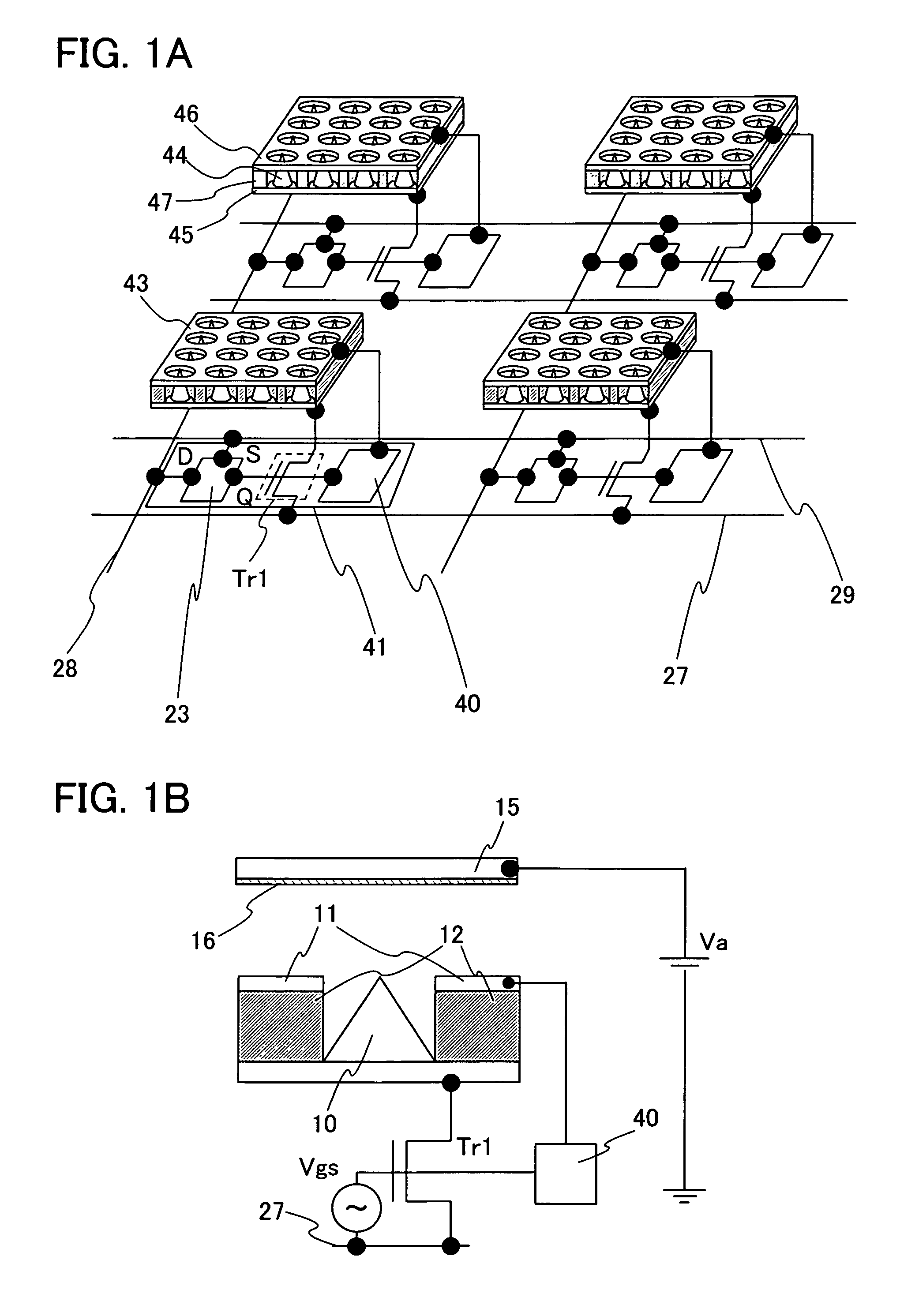
[0088]In this embodiment mode, a display device in accordance with the invention is described with reference to FIGS. 1A and 1B. A display device of the invention includes a plurality of data lines 28, a plurality of scan lines 29 which are provided to be at right angles to the respective data lines, a pixel circuit which is provided in an intersection region (also described as pixel region) of the data lines 28 and the scan lines 29, and light-emitting elements. Each light-emitting element includes an emitter array 43, a fluorescent material, and an anode electrode, and the fluorescent material and the anode electrode are provided on an opposite substrate. The emitter array 43 includes an emitter 44, a cathode electrode which is provided below the emitter, an extraction gate electrode 46 which is provided so as to surround the upper circumference of the emitter, and an insulating material 47 which is provided so as to surround the circumference of the whole emitter to insulate each...
embodiment mode 2
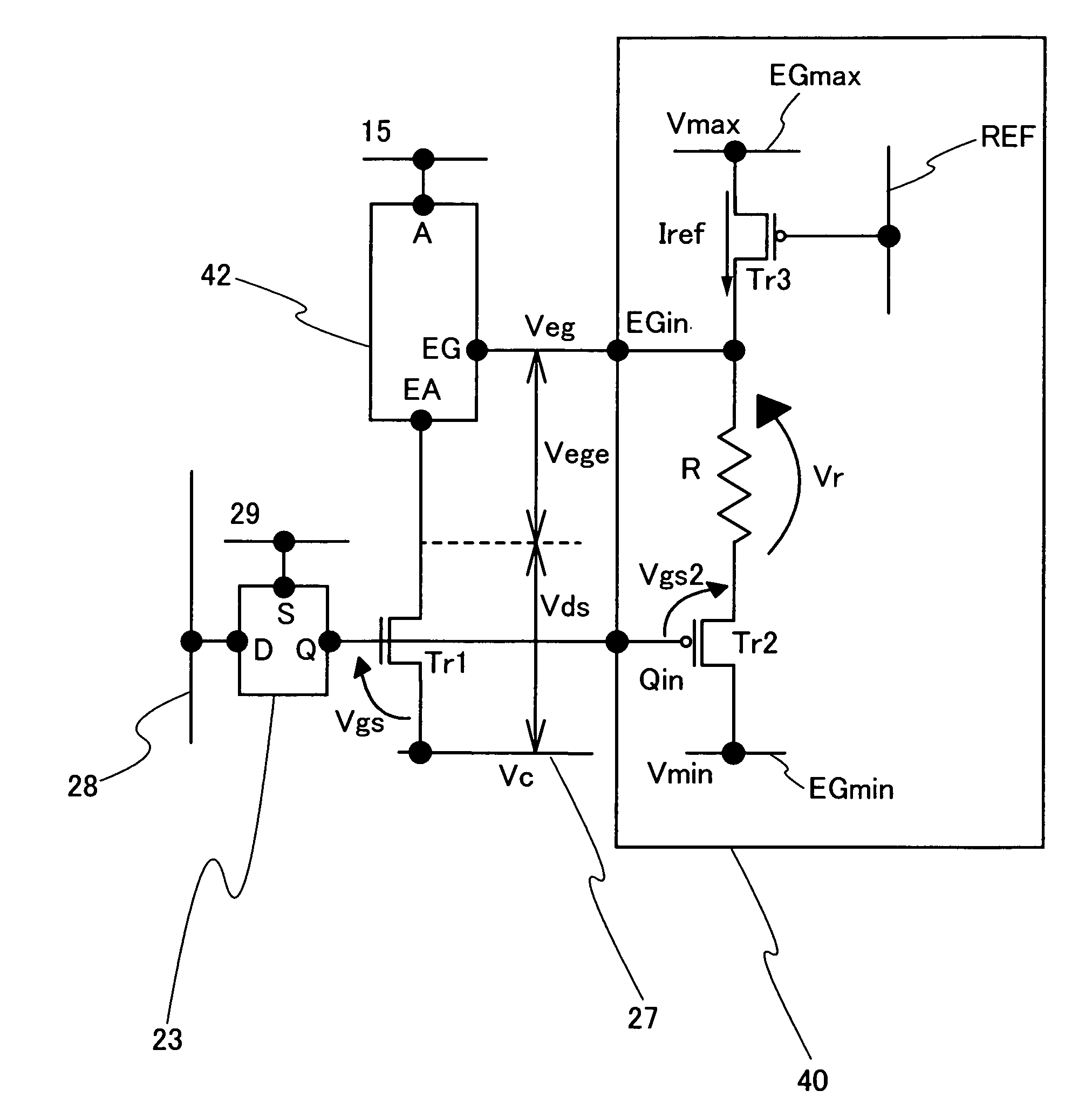
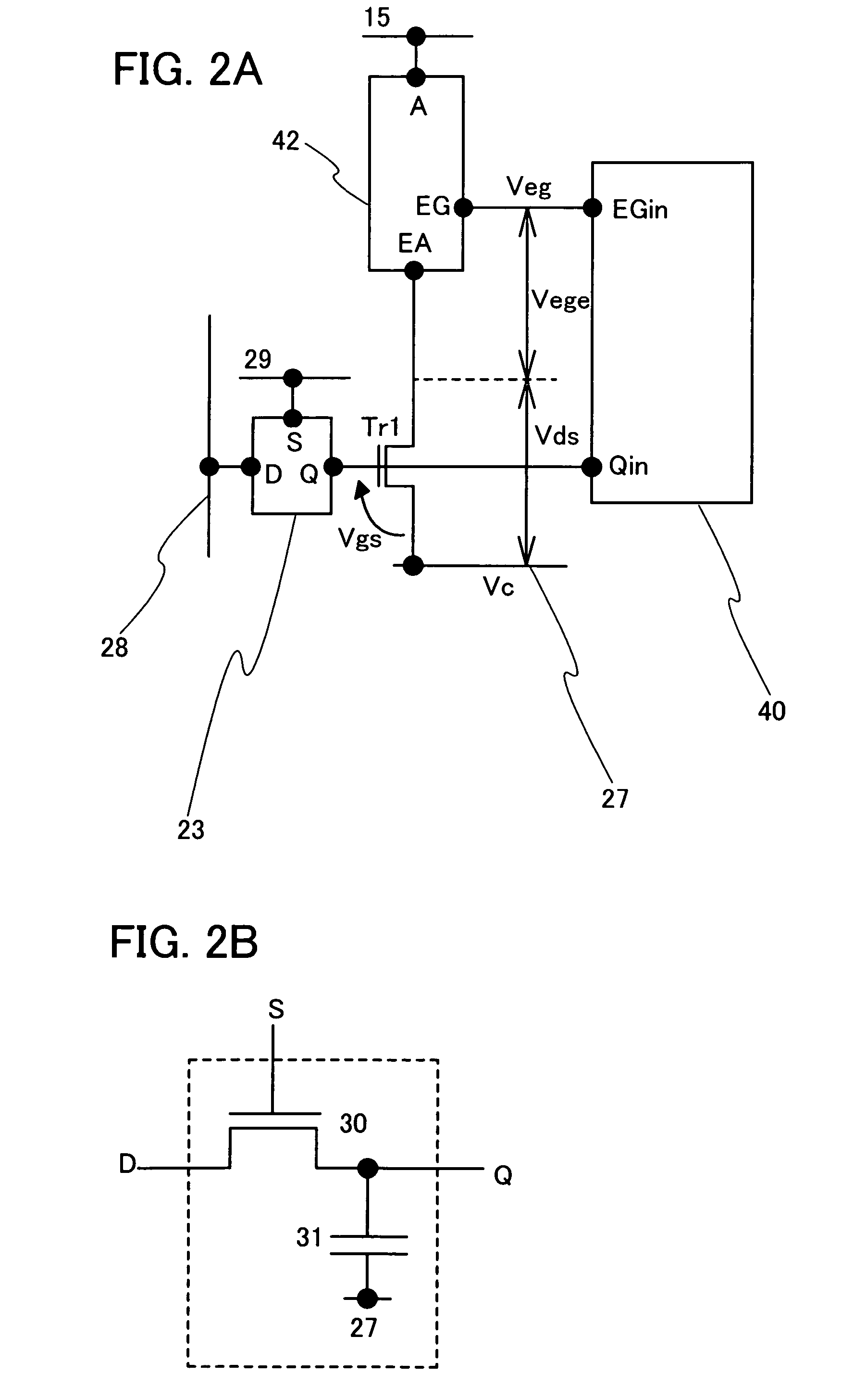
[0115]A display device of the invention includes the potential control circuit 40 of an extraction gate electrode described in Embodiment Mode 1 in a pixel circuit; however, it also includes a gate electrode potential control circuit 23 of a driving transistor in the pixel circuit. Although the invention can be applied to either the case of driving the display device with an analog value and the case of driving it with a digital value, it is particularly preferable in the display device of the invention that the gate electrode potential control circuit 23 of a driving transistor be a circuit which can process analog values, since the potential control circuit 40 of an extraction gate electrode can control the extraction gate electrode 11 of the light-emitting element 42 with analog values even if the gate-source voltage Vgs of the driving transistor Tr1 has an analog value.
[0116]However, electric characteristics of the driving transistor Tr1 vary in each pixel. Then, there is a case...
embodiment mode 3
[0152]In this embodiment mode, description is made of a configuration of the whole display device of the invention. Although various kinds of configurations of the display device of the invention can be considered, here, description is made of an exemplary configuration of the peripheral driver circuit which realizes the operation of the pixel circuit described in Embodiment Mode 2. FIG. 23 shows an exemplary configuration of a display device which includes the pixel circuits described in FIG. 20A, FIG. 21A, or FIG. 22A. A display device described in FIG. 23 includes a pixel portion 90, a control circuit 91, a power supply circuit 92, an image data converter circuit 93, a data line driver 94, and a scan line driver 95. The power supply circuit 92 includes a power supply CV for the control circuit and the image data converter circuit, a power supply DV for the drivers, a high voltage power supply HV, and a power supply PV for the pixel portion. The data line driver 94 includes a shif...
PUM
 Abstract
Description
Claims
Application Information