Operation stabilized pixel bias circuit

a technology of pixel bias circuit and stabilized pixel bias, which is applied in the field of improving the stability of the bias current in the imager, can solve the problems of reducing the output signal, unstable horizontal band-wise noise of one or more pixels, and preventing the cut-off of the bias current, so as to improve the stability of the output. stability, the effect of preventing the cut-o

Active Publication Date: 2010-11-02
APTINA IMAGING CORP
View PDF29 Cites 8 Cited by
  • Summary
  • Abstract
  • Description
  • Claims
  • Application Information

AI Technical Summary

Benefits of technology

[0024]Exemplary embodiments of the method and apparatus of the present invention provide a power source that provides a stabilized pixel bias current supply in an imager. The power source features a current bypass circuit to prevent bias current cut-off from adversely affecting the stability of the output of the power source. The power source also features a voltage limiter to prevent a pixel from outputting an out of range output voltage when very strong light is incident upon the pixel.

Problems solved by technology

In particular, saturation of one or more pixels may manifest in the image produced by the imager 100 as unstable horizontal band-wise noise.
Another problem associated with the above described imager 100 occurs when extremely bright light, such as sunlight, is incident upon the pixel 121.
Thus, a very bright light incident upon a pixel may result in a decrease in the output signal, which ultimately manifests as a negative photoconversion response.

Method used


Image

  • Operation stabilized pixel bias circuit
  • Operation stabilized pixel bias circuit
  • Operation stabilized pixel bias circuit

Examples


first embodiment

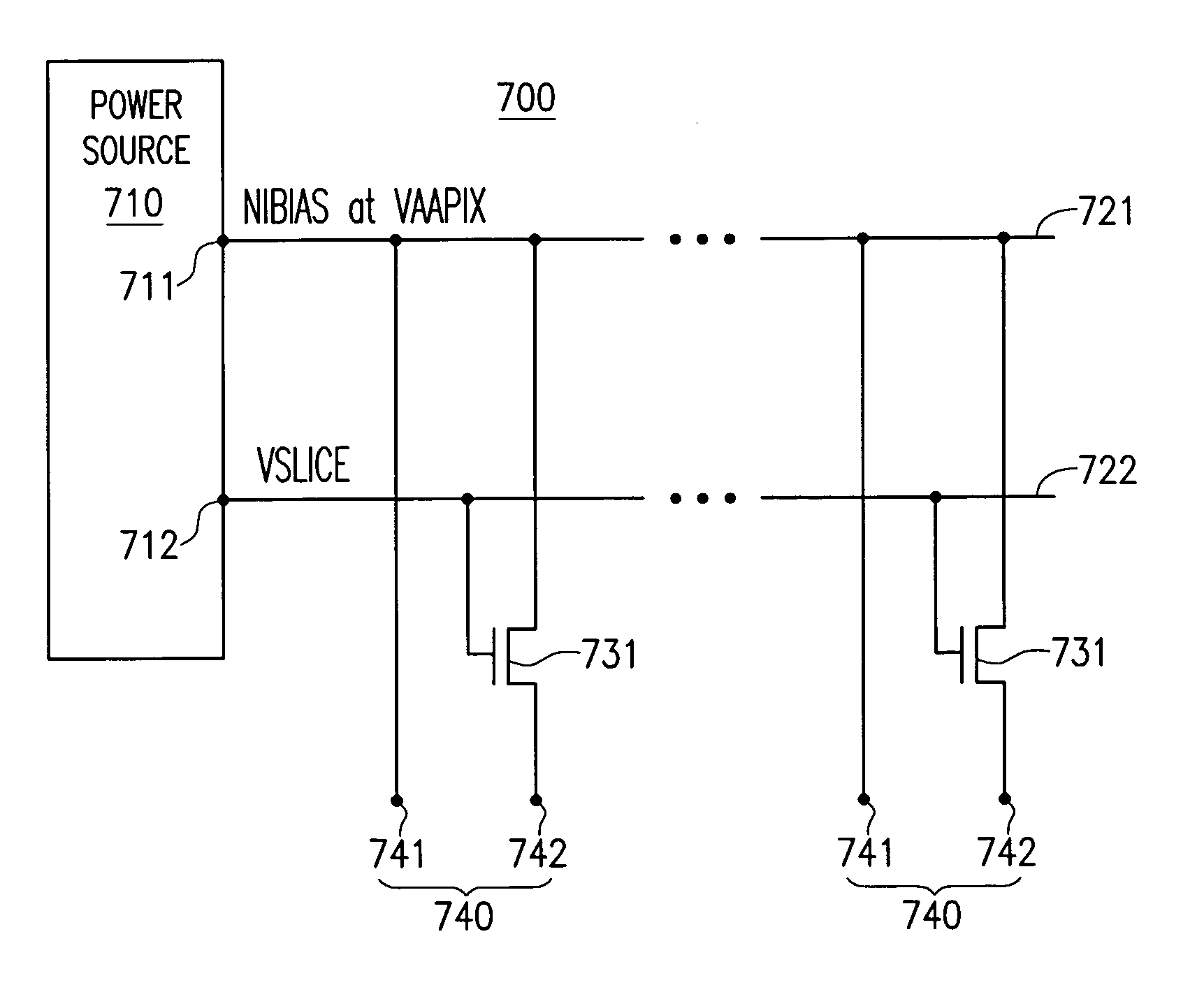
[0043]While the FIG. 7A embodiment of the invention addresses and reduces the unstable horizontal band-wise noise, it does not address the reverse video noise. FIG. 7B is an illustration of a second exemplary embodiment of the present invention, which provides a way to reduce the reverse video noise. The second exemplary embodiment of the present invention utilizes a power source 700′, which is similar to the bias current supply circuit 700 of the first exemplary embodiment. However, circuit 700′ includes a new power source 710′ and is intended to be used with a new control circuit 160′. The power source 710′ is similar to the power source 710 of the first embodiment, but further includes a new control signal input node 713, which accepts a new control signal SLICE_R. The power source 710′ is modified to control the output of the VSLICE control signal based upon the state of the SLICE_R control signal. The SLICE_R is control signal produced by a modified control circuit 160′, which ...

third exemplary embodiment

[0046]Both the unstable load noise and the reverse video noise are addressed by the present invention. The third exemplary embodiment utilizes the same bias current supply circuit 700′ as the second exemplary embodiments (FIG. 7B). Referring now to the supplemental timing diagram of FIG. 9, it can be seen that the VSLICE signal is generally at the VS voltage level. However, when the SLICE_R control signal is asserted, the VSLICE signal is at the higher VR voltage level. By setting the VSLICE signal at the VR voltage level during the reset phase, the reverse video noise is reduced as explained above in connection with the second exemplary embodiment. Similarly, by setting the VSLICE signal at the VS voltage level during the photo signal phase, the unstable load noise is reduced as explained above with respect to the first exemplary embodiment. The third exemplary embodiment therefore combines elements of the first and second exemplary embodiments to address both the unstable load noi...


PUM


Abstract

A pixel bias current supply for supplying a stable source of bias current to pixels of an imager includes a current bypass feature for improving stability when one or more pixels of an imager saturates. The pixel bias current supply also features voltage limiters to restrict the output voltage of a pixel in order to prevent reverse video from being output when very strong light is incident upon one or more pixels.

Description

FIELD OF INVENTION[0001]The present invention relates generally to semiconductor imagers. More specifically, the present invention relates to methods and apparatus for improving bias current stability in an imager.BACKGROUND OF THE INVENTION[0002]FIG. 1 illustrates a conventional imager 100 in block diagram form. As illustrated, the imager 100 includes a power source 110, a pixel array 120 including a plurality of pixels 121, a plurality of load circuits 130, a plurality of sample and hold circuits 140, and a plurality of amplifiers 150. Typically, there are numerous pixels 121 arranged in a plurality of rows and columns. However, for simplicity, the pixel array 120 illustrated in FIG. 1 only includes two columns and one row of pixels 121. The power source 110 produces a bias current IBIAS at an array pixel voltage of VAAPIX. Load circuit 130 produces a bias current IBIAS and this bias current IBIAS is supplied to each pixel 121 of the imager 100. The imager 100 also includes a cont...

Claims


Application Information

Patent Timeline
Patent Type & Authority Patents(United States)
IPC IPC(8): H04N5/217H04N5/225H04N5/359
CPCH04N5/3598H04N25/627
Inventor TAKAYANAGI, ISAO
Owner APTINA IMAGING CORP
Why Eureka
Try Eureka