MOSFET with asymmetrical extension implant

a technology of asymmetrical extension and mosfet, which is applied in the direction of basic electric elements, electrical apparatus, and semiconductor devices, can solve the problems of significant barrier to high drive current and high performance, unexpectedly high external resistance of devices, and unsatisfactory known (110) mosfet devices, etc., and achieve the effect of dramatic reduction of external resistance (rext) of structures

Active Publication Date: 2010-11-09
ADVANCED MICRO DEVICES INC
View PDF10 Cites 5 Cited by
  • Summary
  • Abstract
  • Description
  • Claims
  • Application Information

AI Technical Summary

Benefits of technology

[0005]The present invention relates to a MOSFET structure with asymmetrically implanted source and drain extension regions formed within a substrate (e.g., a Si or SiGe semiconductor-on-insulator substrate) having a (110) surface orientation. An unexpected result of this method is that the external resistance (Rext) of the structure is dramatically reduced.

Problems solved by technology

Known (110) pMOSFET (pMOS, or pFET) devices, however, are unsatisfactory in a number of respects.
For example, such devices exhibit an unexpectedly high source-drain external resistance (Rext).
This resistance penalty substantially limits drive current, in some cases by 20%, and thus presents a significant barrier to achieving high drive current and high performance in (110) PMOS devices.

Method used


Image

  • MOSFET with asymmetrical extension implant
  • MOSFET with asymmetrical extension implant
  • MOSFET with asymmetrical extension implant

Examples


Embodiment Construction

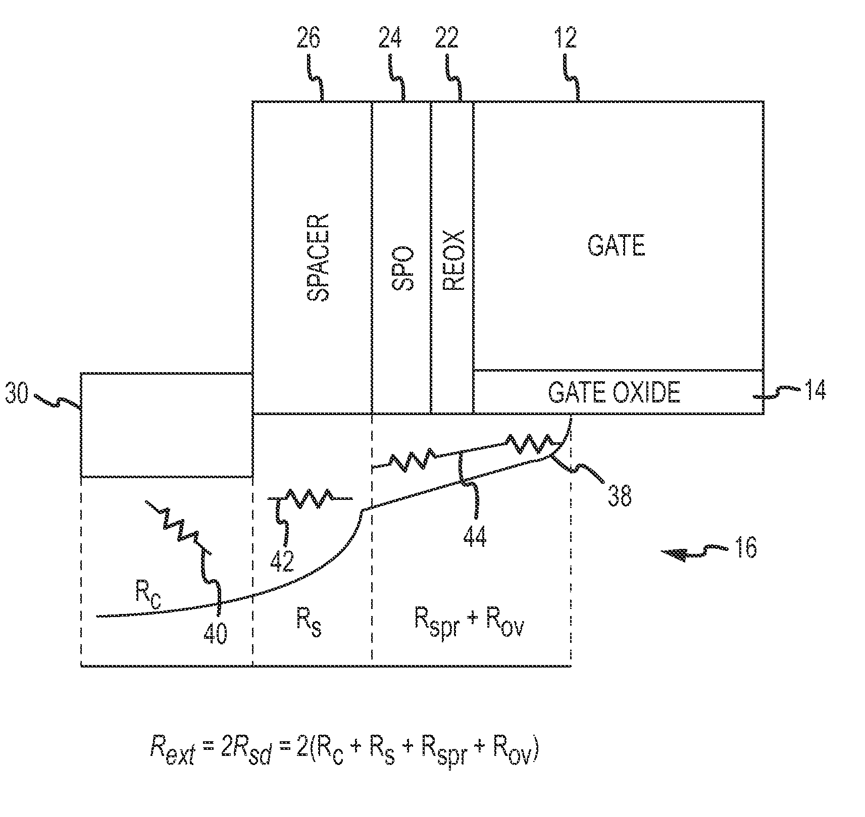
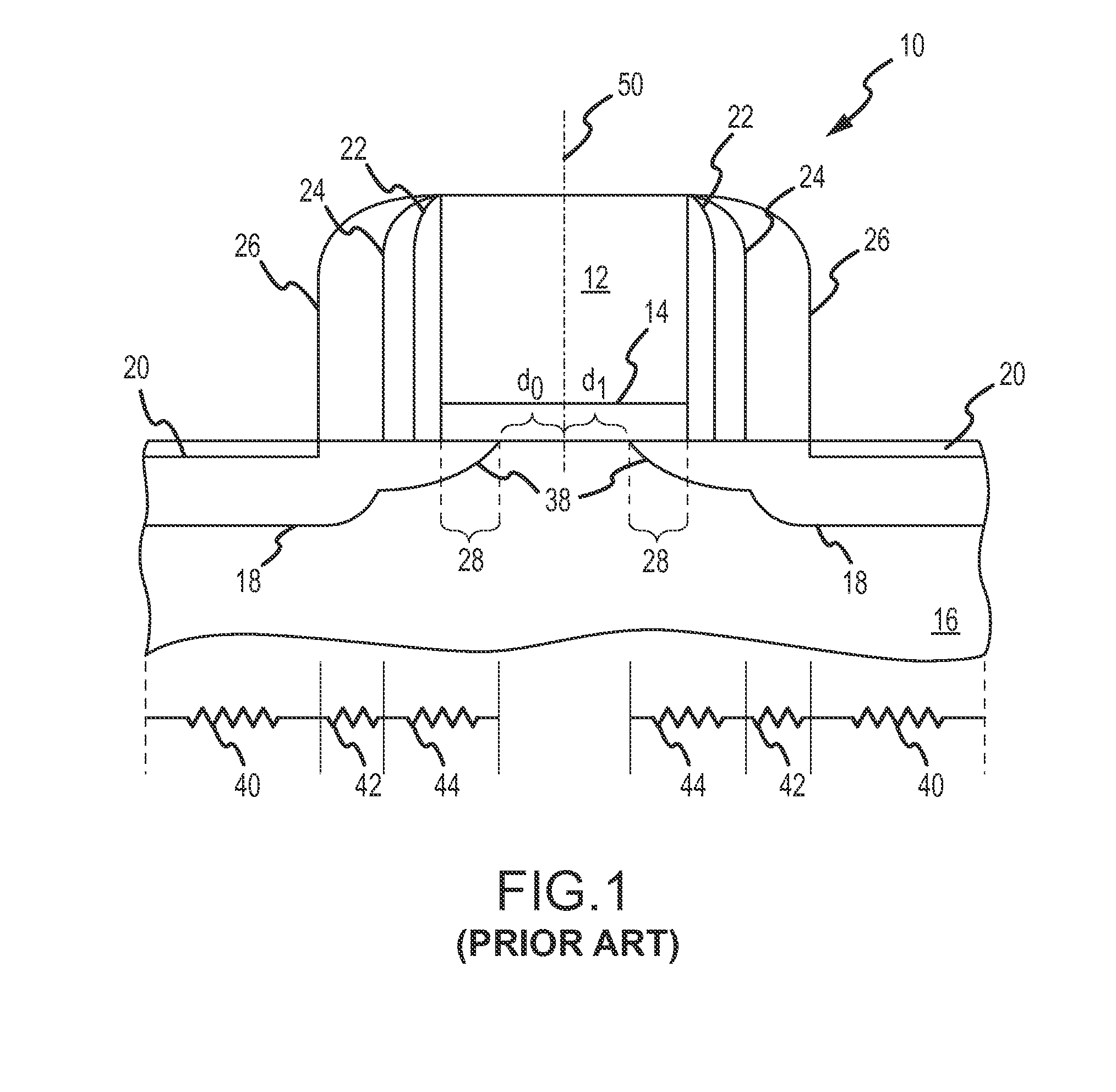
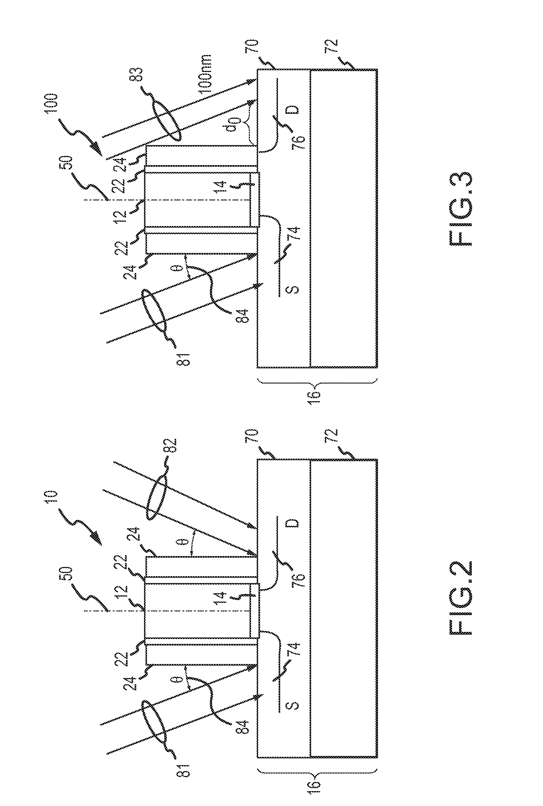
[0019]In general, the present invention relates to (110) channel pFET structures incorporating asymmetrically positioned drain and source extensions that greatly reduce Rext. In this regard, the following detailed description is merely exemplary in nature and is not intended to limit the range of possible embodiments and applications. Furthermore, there is no intention to be bound by any theory presented in the preceding background or the following detailed description.

[0020]For simplicity and clarity of illustration, the drawing figures depict the general structure and / or manner of construction of the various MOSFET embodiments. Elements in the drawings figures are not necessarily drawn to scale: the dimensions of some features may be exaggerated relative to other elements to assist understanding of the exemplary embodiments. In the interest of conciseness, conventional techniques, structures, and principles known by those skilled in the art may not be described herein, including, ...


PUM


Abstract

A method for fabricating a MOSFET (e.g., a PMOS FET) includes providing a semiconductor substrate having surface characterized by a (110) surface orientation or (110) sidewall surfaces, forming a gate structure on the surface, and forming a source extension and a drain extension in the semiconductor substrate asymmetrically positioned with respect to the gate structure. An ion implantation process is performed at a non-zero tilt angle. At least one spacer and the gate electrode mask a portion of the surface during the ion implantation process such that the source extension and drain extension are asymmetrically positioned with respect to the gate structure by an asymmetry measure.

Description

FIELD OF THE INVENTION[0001]The present invention generally relates to MOS structures and methods for fabricating MOS structures, and more particularly relates to improved extension implant configurations for use in (110) channel p-type MOSFET devices, such as planar (110) pMOSFET, FinFET and Tri-gate FETs employing (110) side wall channels.BACKGROUND OF THE INVENTION[0002]There has been an increased interest in metal-oxide-semiconductor field-effect transistors (MOSFETs) incorporating substrates having a (110) surface orientation, particularly with respect to PMOS devices. This interest is due to the increased (approximately 2×) hole mobility advantage as compared to traditional (100) devices as well as the ever-increasing importance of (110) channels in advanced FET structures, such as FinFETs, Tri-gate FETs, and the like.[0003]Known (110) pMOSFET (pMOS, or pFET) devices, however, are unsatisfactory in a number of respects. For example, such devices exhibit an unexpectedly high so...

Claims


Application Information

Patent Timeline
Patent Type & Authority Patents(United States)
IPC IPC(8): H01L21/336H01L21/8234
CPCH01L21/26586H01L29/66659H01L29/7834H01L2924/0002Y10S438/931H01L2924/00
Inventor YANG, FRANK BINWAITE, ANDREW M.LUNING, SCOTT
Owner ADVANCED MICRO DEVICES INC
Why Eureka
Try Eureka