Semiconductor memory device for generating column address

a memory device and memory technology, applied in the direction of information storage, static storage, digital storage, etc., can solve the problems of increasing the access time and difficulty in ensuring an appropriate timing margin, and achieve the effect of sufficient margin and improving the access tim

Active Publication Date: 2010-11-16
SK HYNIX INC
View PDF9 Cites 8 Cited by
  • Summary
  • Abstract
  • Description
  • Claims
  • Application Information

AI Technical Summary

Benefits of technology

[0025]Embodiments of the present invention are directed to providing a semiconductor memory device that can ensure a sufficient margin between a column select signal and a column address even though a delay time of the column select signal is increased to improve an address access time (tAA) during a write operation.

Problems solved by technology

Under the FAST PVT condition, the command signals BWEN and YS sensitive to the PVT variation can be faster than the data signals DATA(GIO), so that it is difficult to ensure an appropriate timing margin tMARGIN.
However, an activation timing of the column select signal YS is intentionally delayed as described above, thus leading to an increase in an address access time (tAA).
Further, if such a situation takes place under the SLOW PVT condition, a delay value of the column select signal YS becomes greater, which may cause the column select signal YS not to fall within the address window valid tWV.

Method used


Image

  • Semiconductor memory device for generating column address
  • Semiconductor memory device for generating column address
  • Semiconductor memory device for generating column address

Examples


Embodiment Construction

[0035]Hereinafter, a semiconductor memory device in accordance with the present invention will be described in detail with reference to the accompanying drawings.

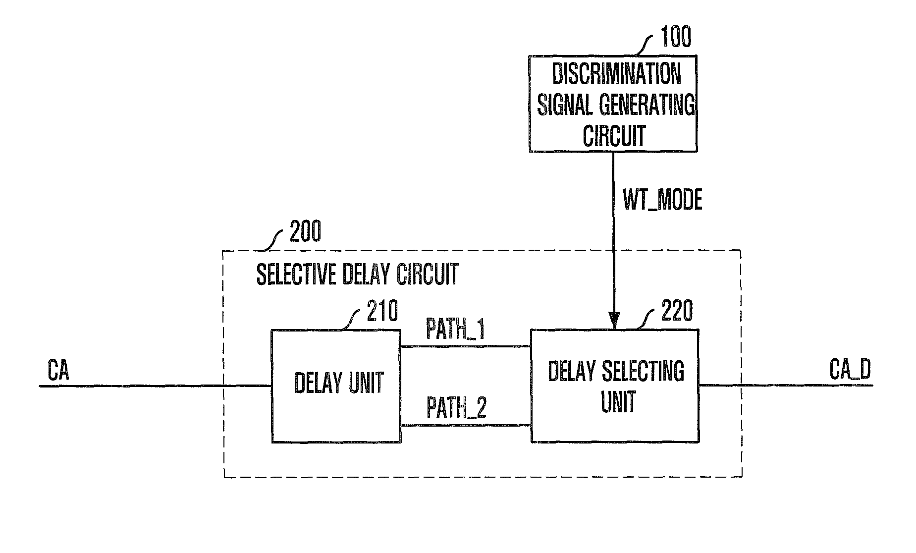
[0036]FIG. 4 is a block diagram illustrating a column address transmission line of a semiconductor memory device in accordance with the invention.

[0037]The semiconductor memory device in accordance with the invention includes a discrimination signal generating circuit 100 and a selective delay circuit 200. The semiconductor memory device changes a delay value of a column address signal CA according to whether a current operation is a write operation or not, thereby increasing a timing margin between the column address signal CA and a column select signal YS.

[0038]The discrimination signal generating circuit 100 generates a discrimination signal WT_MODE indicating that the semiconductor memory device performs a write operation. In the semiconductor memory device of the invention, a delay value of the column address signal CA...


PUM


Abstract

A semiconductor memory device can ensure a sufficient margin between a column select signal and a column address signal when a delay time of the column select signal is increased to improve an address access time during a write operation. The semiconductor memory device includes a discrimination signal generating circuit configured to generate a discrimination signal activated in a write operation of the device, and a selective delay circuit configured to selectively delay a column address in response to the discrimination signal.

Description

CROSS-REFERENCE TO RELATED APPLICATION[0001]The present invention claims priority of Korean patent application number 10-2007-0137428, filed on Dec. 26, 2007, which is incorporated by reference in its entirety.BACKGROUND OF THE INVENTION[0002]The present invention relates to a semiconductor memory device, and more particularly to a semiconductor memory device that can stably ensure a timing margin in generating a column select signal (YS).[0003]FIG. 1 is a block diagram of a conventional semiconductor memory device having eight banks, BANK0, BANK1, BANK2, BANK3, BANK4, BANK5, BANK6 and BANK7.[0004]With the recent development of semiconductor memory devices, having large capacity and high performance, e.g., DDR3 SDRAM, the semiconductor memory devices have changed in configuration from four banks to eight banks.[0005]In a chip of such a semiconductor memory device, data input / output (I / O) pads are called DQ pads, and I / O pads for addresses and commands are called AC pads. Such AC pad...

Claims


Application Information

Patent Timeline
Patent Type & Authority Patents(United States)
IPC IPC(8): G11C7/00
CPCG11C7/22G11C11/4076G11C11/408G11C8/18
Inventor KIM, KYUNG-WHANPARK, EUN-YOUNG
Owner SK HYNIX INC
Why Eureka
Try Eureka