Organic light emitting diode device and method for fabricating the same

Active Publication Date: 2007-07-05
LG DISPLAY CO LTD
View PDF2 Cites 11 Cited by
  • Summary
  • Abstract
  • Description
  • Claims
  • Application Information

AI Technical Summary

Benefits of technology

[0027]Therefore, an object of the present invention is to provide an organic light emitting diode device which can obtain a sufficient margin and expand a design a

Problems solved by technology

However, the liquid crystal display is not a self light emitting device but requires backlight as an external light source.
In addition, the liquid crystal display has technical limits in its brightness, contrast, viewing angle and size.
Especially, unlike a liquid crystal display or a plasma display panel (PDP), the organic electroluminescent device requires only deposition and encapsulation equipment in fabrication.
In the passive matrix method, when the number of the lines increases, a higher voltage and current must be instantaneously ap

Method used


Image

  • Organic light emitting diode device and method for fabricating the same
  • Organic light emitting diode device and method for fabricating the same
  • Organic light emitting diode device and method for fabricating the same

Examples


Embodiment Construction

[0041]Reference will now be made in detail to the preferred embodiments of the present invention, examples of which are illustrated in the accompanying drawings.

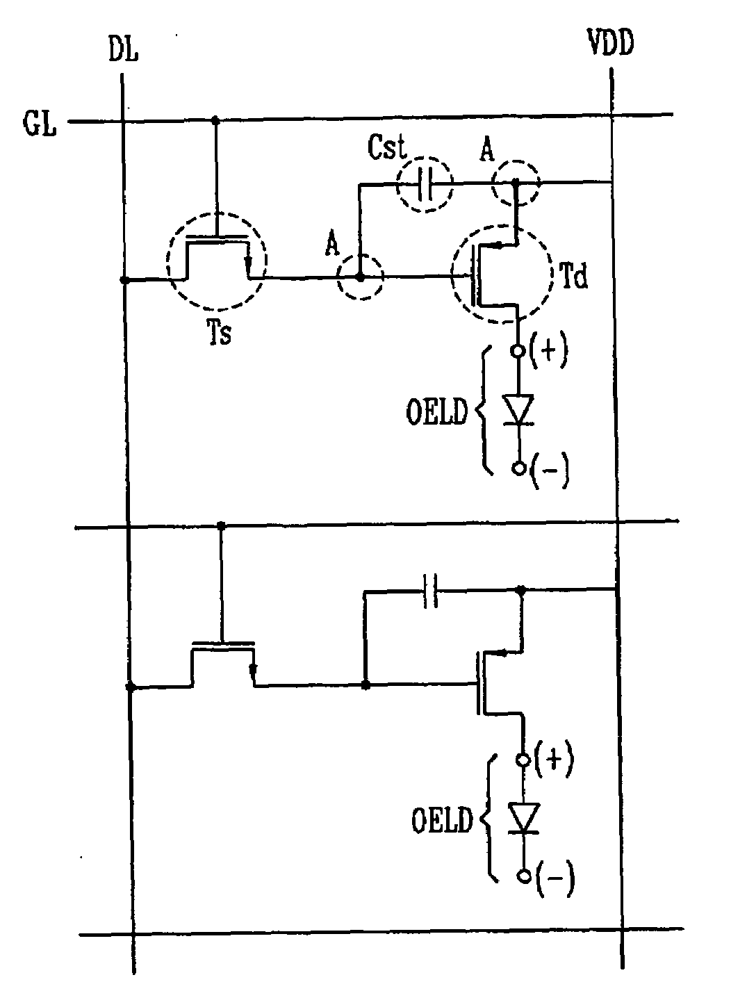
[0042]FIG. 3 is a circuit illustrating a basic structure of a pixel in an active matrix organic light emitting diode device in accordance with an embodiment of the present invention. FIG. 4 is an enlarged layout view illustrating part A of FIG. 3 in the active matrix organic light emitting diode device in accordance with an embodiment of the present invention.

[0043]Referring to FIG. 3, gate lines GL are formed on a substrate (not shown) in a first direction, and a data line DL and a power supply line VDD are formed in a second direction crossing the first direction and isolated from each other at a predetermined interval, for defining one pixel area. A switching TFT Ts which is an addressing element is formed at the crossing point of the gate line GL and the data line DL. A storage capacitor Cst is connected to the switching...


PUM


Abstract

An organic light emitting diode device includes a gate electrode of a first transistor on a substrate; a gate insulation film on the gate electrode of the first transistor; a source electrode of a second transistor on the gate insulation film and overlapping with the gate electrode of the first transistor; a contact hole exposing the gate electrode of the first transistor and the source electrode of the second transistor; a conductive wiring in the contact hole, for electrically connecting the gate electrode of the first transistor and the source electrode of the second transistor.

Description

CROSS-REFERENCE TO RELATED APPLICATION[0001]This Nonprovisional Application claims priority under 35 U.S.C. §119(a) on Patent Application No. 10-2005-0136343 filed in Korea on Dec. 31, 2005, the entire contents of which are hereby incorporated by reference.BACKGROUND OF THE INVENTION[0002]1. Field of the Invention[0003]The present invention relates to an organic light emitting diode device and a method for fabricating the same, and more particularly, to an organic light emitting diode device which can obtain a sufficient margin and expand a design area of a driving transistor, by reducing the number of contact holes to minimize the area occupied by the contact holes, and a method for fabricating the same.[0004]2. Description of the Background Art[0005]A liquid crystal display with the features of light weight and low power consumption has been generally used as a flat panel display (FPD). However, the liquid crystal display is not a self light emitting device but requires backlight ...

Claims


Application Information

Patent Timeline
IPC IPC(8): H01J1/62
CPCH01L27/12H01L27/1248H01L27/124H01L27/3276H10K59/131H05B33/22H05B33/10
Inventor CHOI, HEE-DONGPARK, JAE-HEE
Owner LG DISPLAY CO LTD
Why Eureka
Try Eureka