Electrical contacts for a semiconductor light emitting apparatus

a technology of electrical contacts and light-emitting devices, which is applied in the direction of electrical apparatus, semiconductor/solid-state device manufacturing, and semiconductor devices. it can solve the problems of reducing the light-emitting area and high operating current, and achieve the effect of facilitating supplying current and facilitating supplying curren

Active Publication Date: 2010-11-30
PHILIPS LUMILEDS LIGHTING CO LLC
View PDF7 Cites 16 Cited by
  • Summary
  • Abstract
  • Description
  • Claims
  • Application Information

AI Technical Summary

Benefits of technology

[0025]The structure may include an interconnect between the electrical via contact and at least the first and the second contacts, the interconnect being operable to facilitate supplying current to the first layer.
[0026]Each elongate electrical contact may include a channel having sidewalls and a bottom wall, the sidewalls extending through the second layer and the active layer, the bottom wall comprising a portion of the first layer, an electrically conductive material in the channel and in electrical contact with the first layer, and a dielectric material between the electrically conductive material and the sidewalls, the dielectric material being operable to prevent electrical contact to the second layer and the active layer by the first and second contacts.
[0027]The structure may include an interconnect between at least the first and the second contacts, the interconnect being operable to facilitate supplying current to the first layer.

Problems solved by technology

Additionally demands for increased light output from LEDs are growing resulting in higher operating currents.
However, employing a plurality of contacts may reduce the light generating area of the LED and thus in general, electrical contact design in LEDs involves a trade-off between current spreading and usable light generating area remaining once the contacts have been formed.

Method used


Image

  • Electrical contacts for a semiconductor light emitting apparatus
  • Electrical contacts for a semiconductor light emitting apparatus
  • Electrical contacts for a semiconductor light emitting apparatus

Examples


Embodiment Construction

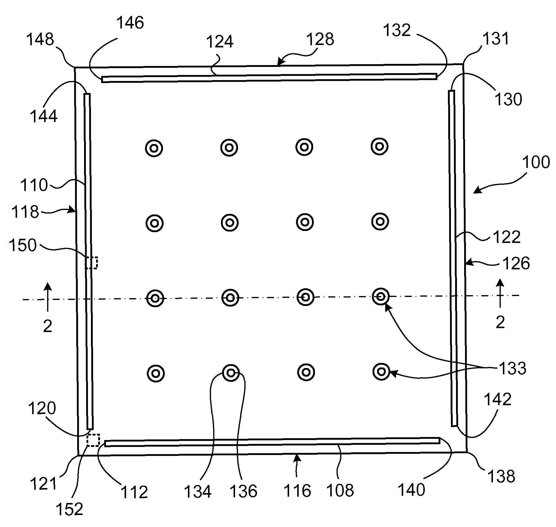
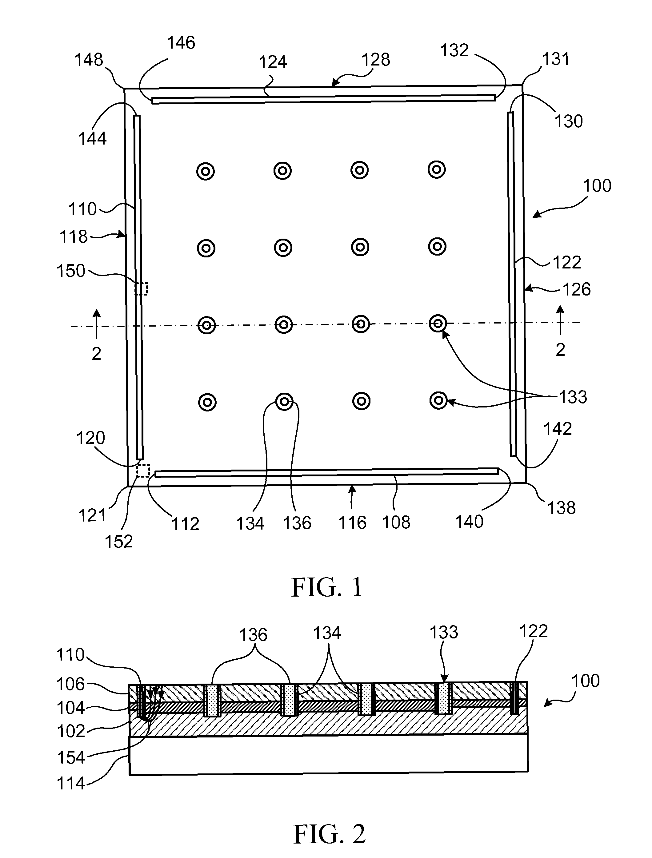
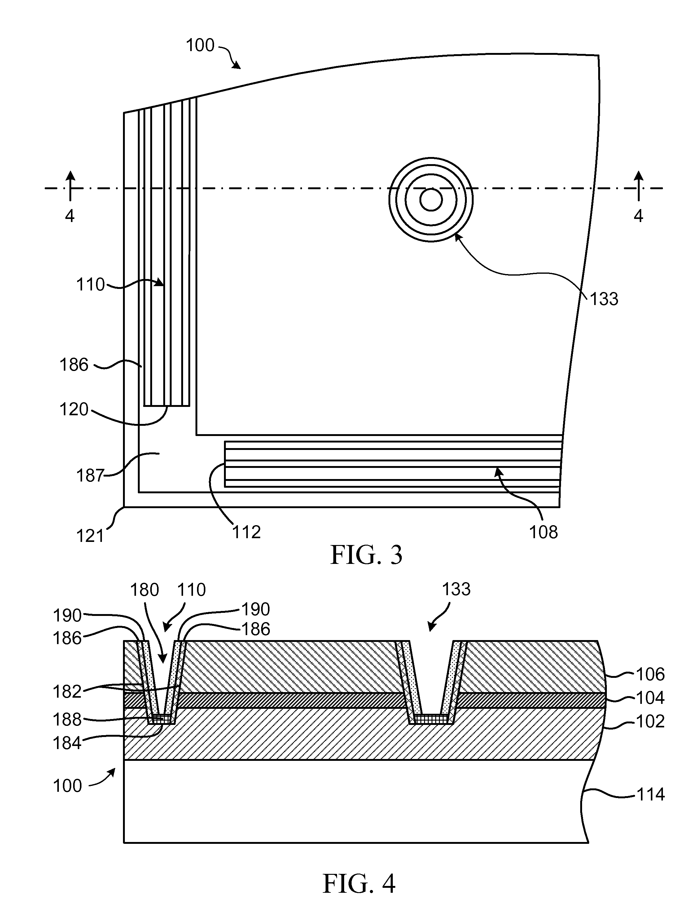
[0042]Referring to FIG. 1 and FIG. 2, a semiconductor structure for use in a semiconductor light emitting apparatus is shown generally at 100. The structure 100 includes a first layer 102 of first conductivity type and an active layer 104 overlying the first layer 102. The active layer 104 is operable to generate light. The structure 100 also includes a second layer 106 of second conductivity type, overlying the active layer 104.

[0043]The structure 100 further includes at least a first elongate electrical contact 108 and a second elongate electrical contact 110 extending through the second layer 106 and the active layer 104, and in electrical contact with the first layer 102. The first and second contacts 108 and 110 are oriented at an angle to each other and the first contact has a first end 112 in proximity with the second contact. The first end 112 is sufficiently spaced apart from the second contact 110 such that when current is supplied to the first layer 102 through the contac...


PUM


Abstract

A process for forming electrical contacts for a semiconductor light emitting apparatus is disclosed. The light emitting apparatus has a first layer of first conductivity type, an active layer for generating light overlying the first layer, and a second layer of second conductivity type overlying the active layer. The process involves forming at least a first and a second elongate electrical contact through the second layer and the active layer to provide electrical connection to the first layer, the first and second contacts oriented at an angle to each other, the first contact having a first end in proximity with the second contact, the first end being sufficiently spaced apart from the second contact such that when current is supplied to the first layer through the contacts, current contributions from the first end of the first contact and the second contact in an area generally between the first end and the second contact cause a current density in the area that is approximately equal to a current density elsewhere along the first and second contacts.

Description

BACKGROUND OF THE INVENTION[0001]1. Field of Invention[0002]This invention relates generally to semiconductor light-emitting devices, and more specifically to electrical contacts for semiconductor light-emitting devices.[0003]2. Description of Related Art[0004]Semiconductor light-emitting devices such as light-emitting diodes (LEDs) provide efficient sources of light and are more robust than incandescent light bulbs and fluorescent tubes. Advancements in LED technology and processing have facilitated the use of such devices as replacements for traditional lighting sources in commercial and residential lighting applications, for example. Efficiency and reliability are thus important aspects of LEDs used in lighting applications. Additionally demands for increased light output from LEDs are growing resulting in higher operating currents.[0005]It is common to fabricate LEDs with both n-type and p-type contacts on the same side of the semiconductor die, such that light may be emitted fr...

Claims


Application Information

Patent Timeline
Patent Type & Authority Patents(United States)
IPC IPC(8): H01L33/62H01L33/20H01L33/38
CPCH01L33/382H01L33/20
Inventor SCHIAFFINO, STEFANOUEBBING, JOHN JULIAN
Owner PHILIPS LUMILEDS LIGHTING CO LLC
Why Eureka
Try Eureka