

Wafer level chip scale package
- Summary
- Abstract
- Description
- Claims
- Application Information
AI Technical Summary
Benefits of technology
Problems solved by technology
Method used
Image

Examples
embodiments
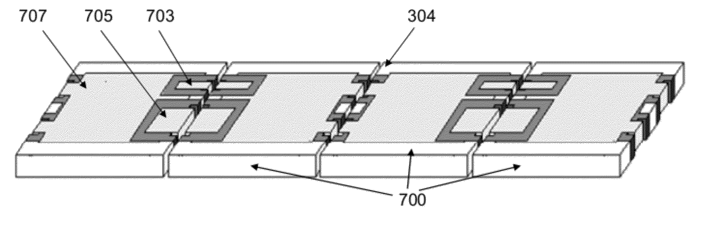
[0022]In embodiments of the present invention, these disadvantages can be overcome by a semiconductor device having a semiconductor substrate with first and second surfaces and a sidewall between them. First and second conductive pads on the first and second surfaces are in electrical contact with corresponding first and second semiconductor device structures in the substrate. A notch is formed on the sidewall running from the first surface to the second surfaces. An insulator layer on the first surface and sidewall of the notch covers a portion of the first conductive pad on the first surface and covers the sidewall of the semiconductor substrate. An electrically conductive layer on part of the insulator layer on the first conductive pad and sidewall is in electrical contact with the second conductive pad. The insulator layer prevents the conductive layer from making electrical contact between the first and second conductive pads, and between the electrodes and the semiconductor su...
PUM
 Abstract
Description
Claims
Application Information