HVNMOS/HVPMOS switched capacitor charge pump having ideal charge transfer

a charge pump and capacitor technology, applied in the direction of electric variable regulation, non-denominational number representation computation, analog and hybrid computing, etc., can solve the problems of large on-resistance and charge current loss, and achieve the effect of reducing the on-resistance of the main switch

Active Publication Date: 2010-11-30
DIALOG SEMICONDUCTOR GMBH
View PDF16 Cites 8 Cited by
  • Summary
  • Abstract
  • Description
  • Claims
  • Application Information

AI Technical Summary

Benefits of technology

[0012]It is an object of at least one embodiment of the present invention to provide a method and a circuit to minimize the On-resistance of the main switch of the charge stage and the pump stage of the present invention.
[0013]It is another object of the present invention to eliminate dynamic currents flowing through the drain-to-substrate and source-to-substrate of each main switch when it switches ON or OFF.
[0014]It is yet another object of the present invention to assure that no current flows through the bulk switches.
[0016]These and other objects have been furthermore achieved by reducing the main switch from two transistors to one transistor, thereby reducing the chip real estate area and their On-resistance. The dynamic current flow is eliminated by synchronously switching the bulk of the main switch to the higher voltage node (source or drain) of the HVPMOS transistor to assure that the bulk voltage is larger than or equal to the source voltage and larger than or equal to the drain voltage. This increased bias of the bulk of the main switches increases their threshold voltage (VT) and thus avoids a current loss during the charge transfer.

Problems solved by technology

This circuit, however, uses two transistors in series which has the above mentioned problems of a large on-resistance and charge current losses.

Method used


Image

  • HVNMOS/HVPMOS switched capacitor charge pump having ideal charge transfer
  • HVNMOS/HVPMOS switched capacitor charge pump having ideal charge transfer
  • HVNMOS/HVPMOS switched capacitor charge pump having ideal charge transfer

Examples


Embodiment Construction

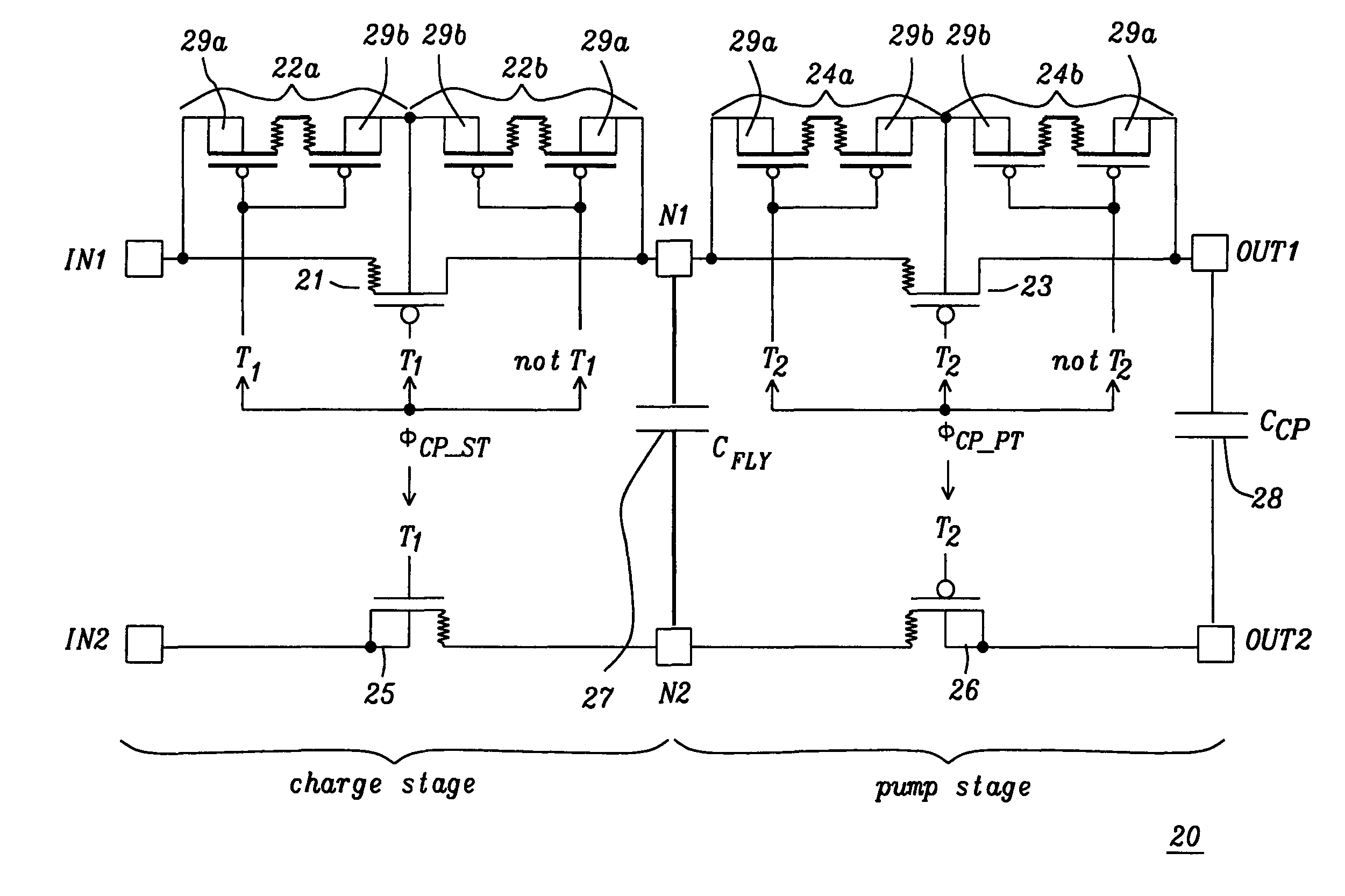
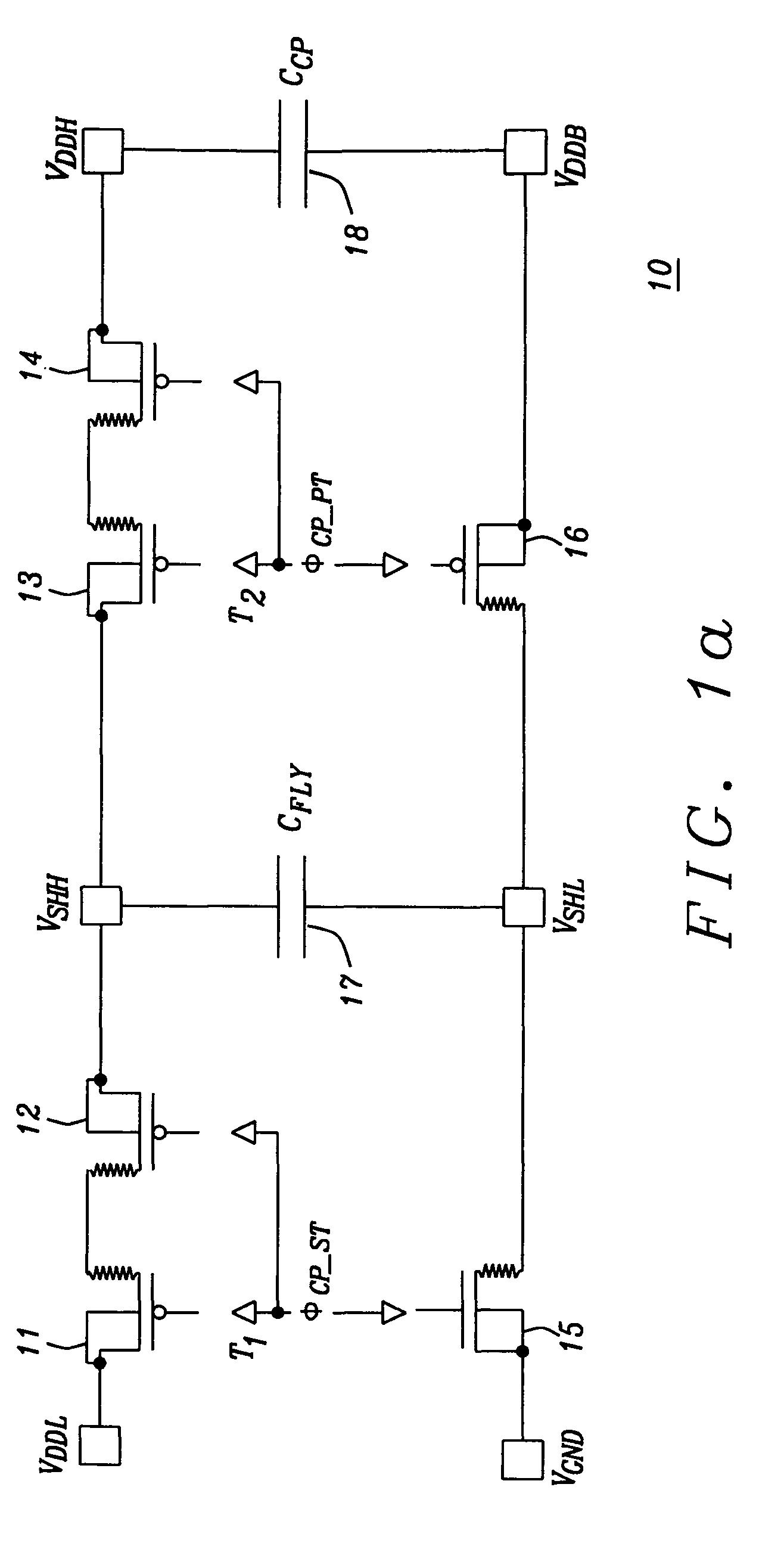
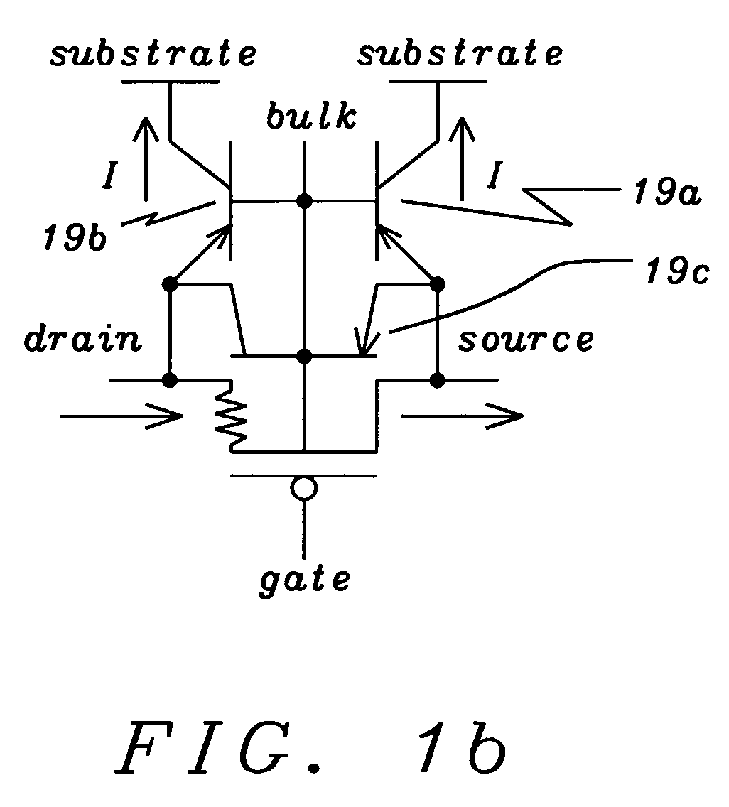
[0028]Previously realized high voltage charge pumps are using two CMOS HVPMOS (High Voltage PMOS) transistors in series as a switch where the bulk of each HVPMOS transistor is connected to its source to avoid turn-on of the parasitic bipolar transistors of each HVPMOS transistor because of the body effect. However, the on-resistance of the switch is large, given by its area W*L of HVPMOS transistors connected series. In addition, there are charge current losses due to dynamic current flowing through the drain to the substrate when VB is less than VD (VBD) when the transistor switches on / off.

[0029]Referring now to FIG. 1a, we describe a charge pump 10 of a technique known to the inventor. HVPMOS transistors 11 and 12 are coupled in series between input VDDL and node VSHH. HVPMOS transistors 13 and 14 are coupled in series between node VSHH and output VDDH. HVNMOS (High Voltage NMOS) transistor 15 is coupled between input VGND and node VSHL, and HVPMOS transistor 16 is coupled between...


PUM


Abstract

An integrated circuit for a charge pump with a charge stage and a pump stage and a single High-Voltage PMOS (HVPMOS) transistor as the main switch for each stage and two times two minimum HVPMOS transistors in series as a bulk switch with fixed bulk connections, where the minimum HVPMOS transistors are smaller sized transistors than the transistors of the main switch. The bulk of the main switch is switched synchronously to the voltage node of the HVPMOS transistor of the main switch to force the bulk voltage (VB) to be equal or larger than either the source voltage (VS) or the drain voltage (VD). Two non-overlapping clock signals are used to trigger the HVPMOS transistors of the charge and pump stage.

Description

BACKGROUND OF THE INVENTION[0001]1. Field of the Invention[0002]The invention relates to an integrated circuit charge pump, and more particularly to a charge pump with a single HVPMOS transistor as a main switch having coupled in parallel to its source and extended drain a bulk switch with fixed bulk connection.[0003]2. Description of the Related Art[0004]Reference is made to A New Charge Pump Without Degradation in Threshold Voltage Due to Body Effect by Jongshin Shin, In-Young Chung, Young June Park, and Hong Shick Min in the IEEE Journal of Solid-State Circuits, Vol. 35, No. 8, August 2000.[0005]U.S. Patent Application 2005 / 0088220 (Hahn et al.) discloses a charge pump circuit which alleviates the body effect of a charge transfer transistor, thereby improving the charge transfer efficiency of the charge transfer transistor. This circuit, however, uses two transistors in series which has the above mentioned problems of a large on-resistance and charge current losses.[0006]U.S. Pat...

Claims


Application Information

Patent Timeline
Patent Type & Authority Patents(United States)
IPC IPC(8): G05F1/10
CPCH02M3/07H02M3/073H02M2003/078H02M3/078
Inventor JI, CANG
Owner DIALOG SEMICONDUCTOR GMBH
Why Eureka
Try Eureka