UV treatment for carbon-containing low-k dielectric repair in semiconductor processing

a technology of low-k dielectric and uv treatment, which is applied in the direction of semiconductor/solid-state device manufacturing, basic electric elements, electric apparatus, etc., can solve the problems of inherently weak nature of low-k dielectric material that can pose significant challenges to downstream electronic-packaging process and material compatibility, host of process integration and material compatibility difficulties, and achieve the effect of reducing the energy of film

Active Publication Date: 2010-12-14
NOVELLUS SYSTEMS
View PDF174 Cites 432 Cited by
  • Summary
  • Abstract
  • Description
  • Claims
  • Application Information

AI Technical Summary

Benefits of technology

[0014]While the invention is not limited to this theory of operation, it is believed that damage sites, including dangling Si bonds and / or highly strained bonds (e.g., Si—O—Si or Si—CH2—Si) in the carbon-containing dielectric film are satisfied with a methyl group from methyl-containing molecules of the gas phase source of methyl (—CH3) groups in a reaction induced by the activation provided by UV radiation, thereby accomplishing low-k dielectric repair without substantial alteration of dielectric properties. In some instances, active methyl (—CH3) groups may be generated by dissociation of methyl-containing molecules of the gas phase source of —CH3 groups by the UV radiation. Alternatively, methyl groups in methyl-containing molecules in the gas phase source of —CH3 groups can react with damage sites in the film. The reaction of the activated methyl groups with the damaged area of the film when the activation energy is lowered by the UV radiation reduces the energy of film, rendering it more stable.

Problems solved by technology

The inherently weak nature of the low-k dielectric material can pose significant challenges for downstream electronic-packaging processes and material compatibility.
This introduces a host of process integration and material compatibility difficulties.
The balance between maintaining the film's integrity and integrating it properly and performing the necessary stripping, cleaning, and conditioning gets increasingly precarious.
The properties that give carbon-containing low-k dielectric materials their desirable low dielectric constants are the very same properties that are leading to significant integration challenges.
Because of the mechanical weakness, carbon-containing low-k films are susceptible to kinetic plasma damage that can undesirably densify the film and thus increase the film's effective k value.
The susceptibility of carbon-containing low-k materials to plasma modification poses a serious integration challenge since plasma processes are routinely used to etch, clean, and deposit films in the manufacturing of a semiconductor device.
Moreover, in damascene processing, prior to metal barrier deposition, process induced carbon-containing low-k dielectric damage can be incurred from etch, dry resist strip, wet cleaning and dry cleaning.
Carbon-containing low-k materials are also susceptible to the intercalation of plasma species, residues, solvents, moisture, and precursor molecules that can either adsorb into, outgas from, or chemically modify the film.
Damage to the carbon-containing low-k dielectric material on the sidewalls of the via trenches or in the inter-layer dielectric (ILD) regions during copper (Cu) damascene processing can compromise the integrity of dielectric spacing, leading to increased leakage, higher capacitance, and reduced performance and reliability.
This can oxidize the barrier material leading to Cu diffusion.
Damage of the low-k dielectric material is linked to the loss of methyl groups (CH3) in the film during processing.
However, both methods narrow the required process window and lead to higher manufacturing costs.

Method used


Image

  • UV treatment for carbon-containing low-k dielectric repair in semiconductor processing
  • UV treatment for carbon-containing low-k dielectric repair in semiconductor processing
  • UV treatment for carbon-containing low-k dielectric repair in semiconductor processing

Examples


Embodiment Construction

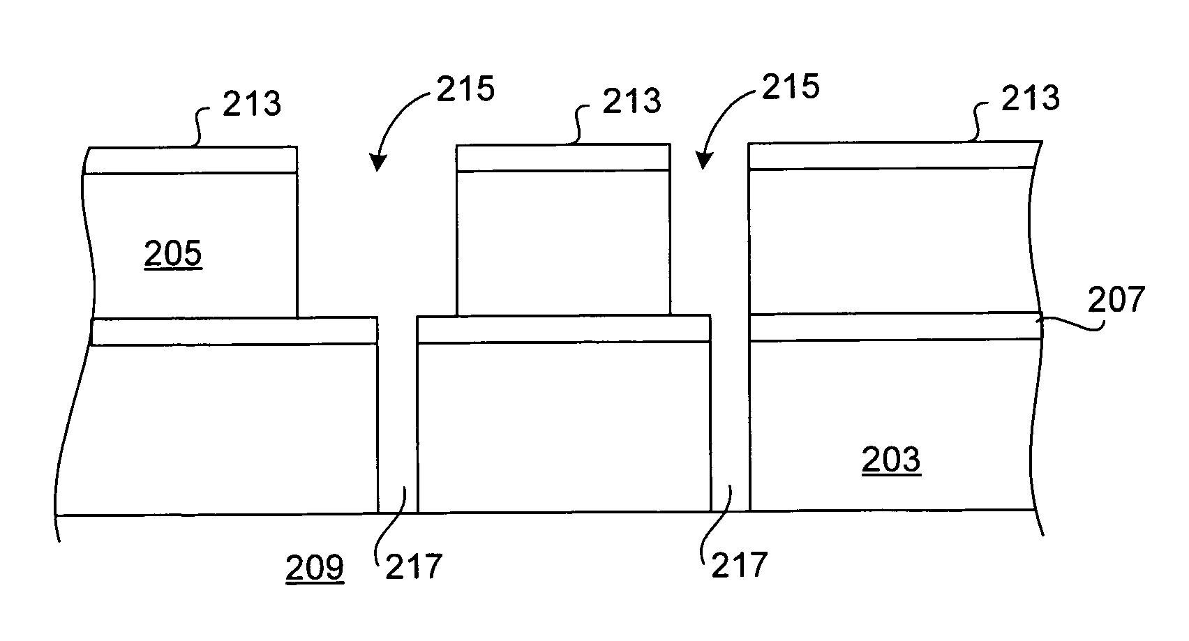
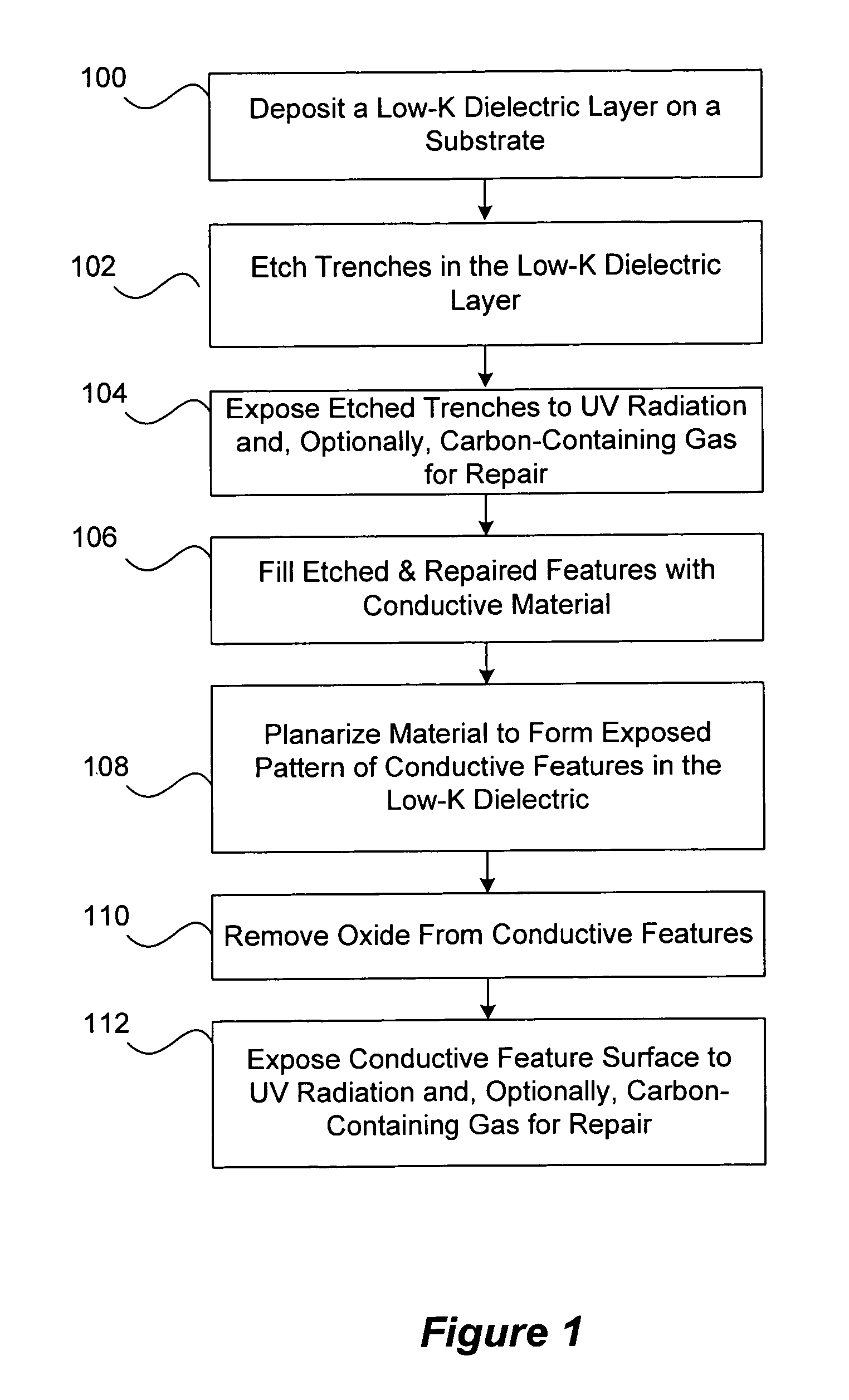
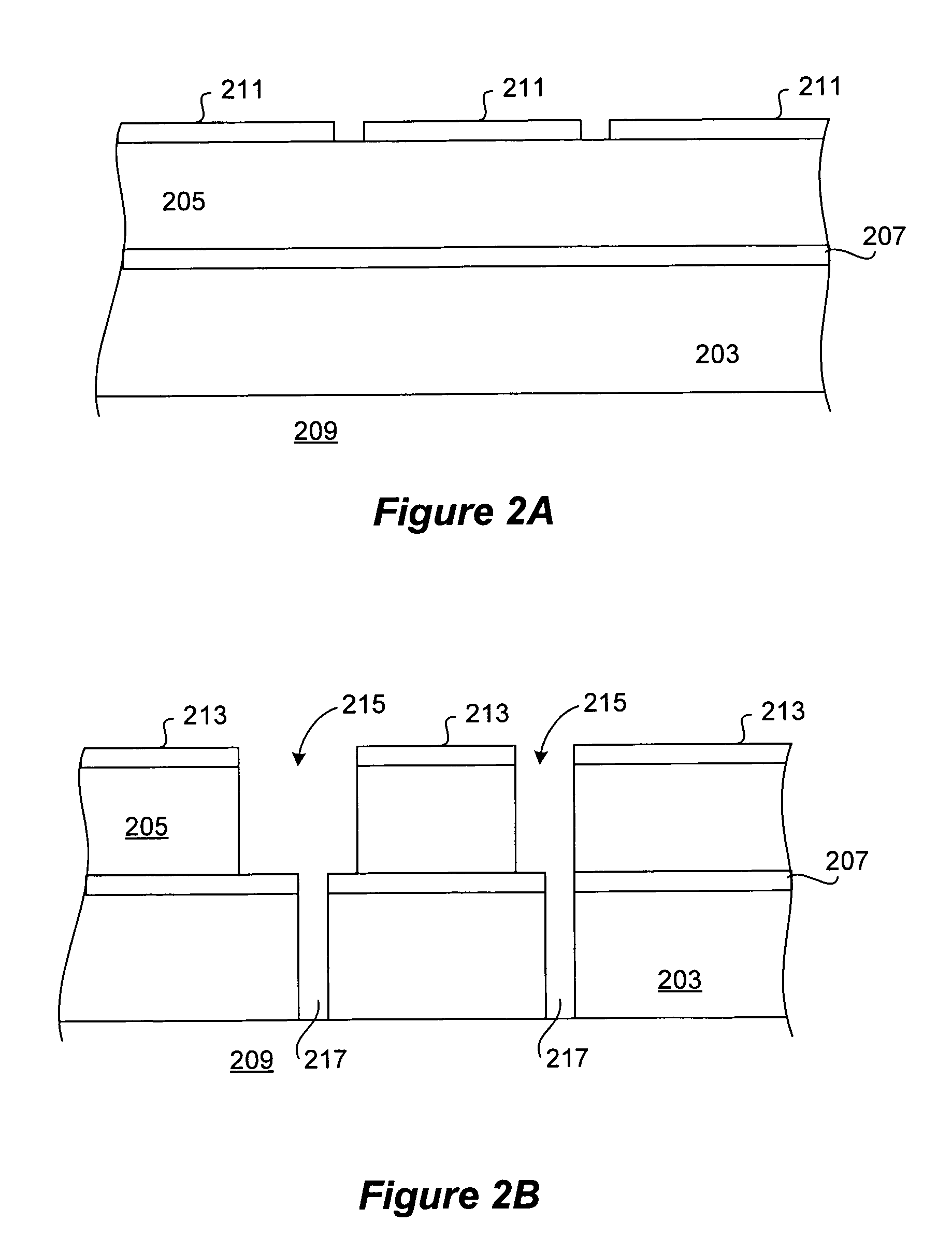
[0024]Embodiments of the present invention are described herein in the context of a UV treatment for carbon-containing low-k dielectric repair in damascene processing. Those of ordinary skill in the art will realize that the following detailed description of the present invention is illustrative only and is not intended to be in any way limiting. Other embodiments of the present invention will readily suggest themselves to such skilled persons having the benefit of this disclosure. Reference will now be made in detail to implementations of the present invention as illustrated in the accompanying drawings. The same reference indicators will be used throughout the drawings and the following detailed description to refer to the same or like parts.

[0025]The term “semiconductor device” as used herein refers to any device formed on a semiconductor substrate or any device possessing a semiconductor material. In many cases, a semiconductor device participates in electronic logic or memory, ...


PUM


Abstract

A method for the ultraviolet (UV) treatment of carbon-containing low-k dielectric enables process-induced damage repair. The method is particularly applicable in the context of damascene processing. A method provides for forming a semiconductor device by depositing a carbon-containing low-k dielectric layer on a substrate and forming a trench in the low-k dielectric layer, the trench having sidewalls ending at a bottom. The trench is then exposed to UV radiation and, optionally a gas phase source of —CH3 groups, to repair damage to the carbon-containing low-k material of the trench sidewalls and bottom caused by the trench formation process (generally etching, ashing, and wet or dry cleaning). A similar treatment, with or without the gas phase source of —CH3 groups, may be applied to repair damage caused in a subsequent planarization operation.

Description

BACKGROUND OF THE INVENTION[0001]The invention relates to low dielectric constant layers in semiconductor processing for use in various applications. More specifically, the invention relates to the UV treatment for repair of process-induced damage of low dielectric constant dielectric materials in, for example, damascene processing.[0002]Ultrafine feature sizes and high performance requirements have necessitated the integration of low dielectric constant (low-k) insulating materials, that are mechanically weaker than previous generation materials, into semiconductor devices. The inherently weak nature of the low-k dielectric material can pose significant challenges for downstream electronic-packaging processes and material compatibility.[0003]Low-k materials are, by definition, those semiconductor-grade insulating materials that have a dielectric constant (“k”) lower than that of SiO2, i.e., 3.9. Various types of low-k materials can have dielectric constants ranging from about 3.8-3...

Claims


Application Information

Patent Timeline
Patent Type & Authority Patents(United States)
IPC IPC(8): H01L21/00
CPCH01L21/3105H01L21/76814H01L21/76825
Inventor VAN SCHRAVENDIJK, BARTCREW, WILLIAM
Owner NOVELLUS SYSTEMS
Why Eureka
Try Eureka