Methods to mitigate plasma damage in organosilicate dielectrics using a protective sidewall spacer

a technology of organosilicate dielectrics and sidewalls, which is applied in the direction of semiconductor devices, semiconductor/solid-state device details, electrical apparatus, etc., can solve the problems of increasing the width of the line trench, the overall speed of the advanced semiconductor chip approaching a limit, and the increase of the line width of the trench, so as to reduce the increase of the line width of the metal trench, the effect of plasma damage reduction

Inactive Publication Date: 2009-03-19
GLOBALFOUNDRIES INC
View PDF8 Cites 197 Cited by
  • Summary
  • Abstract
  • Description
  • Claims
  • Application Information

AI Technical Summary

Benefits of technology

[0036]The present invention addresses the needs described above by minimizing plasma damage to low k and ultra low k organosilicate intermetal dielectric layers. The reduction of the plasma damage is effected by interrupting the etch and strip process flow at a suitable point to add an inventive protective spacer. Optional densification treatment may b...

Problems solved by technology

With the progress in the semiconductor device technology leading to ultra large scale integration, the overall speed of operation of the advanced semiconductor chips is approaching a limit due to signal propagation delay in interconnection wires, which are employed as the high speed interconnect structures, between the individual semiconductor devices on the same advanced semiconductor chip.
Absence or degradation of the metal to metal contact results in low electrical yield.
This results in an increase in the width of the line trench.
This lithographic constraint becomes a particularly challenging problem in the construction of high performance, high density metal interconnects in which fine line widths are required and porous ultra low dielectric constant IMD materials are employed since increased porosity renders the ultra low dielectric constant IMD materials prone to significant plasma damage, and consequently, a significant incremental change from the first width W′ to the second width W″.
Although a tunable range of k values is possible with this set of very low k materials, there are several difficulties in integrating these materials with copper interconnects in a dual damascene process sequence described above or by any other variation of the dual damascene process sequence.
The main difficulty is that the organosilicates are very sensitive to a plasma exposure because of the relative ease of oxidation or cleavage of the Si-organic group linkage (for example, Si-methyl) which results in formation of silanol (Si—OH) groups in the film through a reaction with moisture in the ambient atmosphere.
Silanols further absorb moisture and hence increase the dielectric constant and the dielectric loss factor of the film significantly, thus negating the performance benefits expected from the very low k material.
Silanols also increase the electrical leakage in the very low k material, and thus create a potentially unreliable interconnect structure.
Since reactive ion etch and plasma etch are key steps required in the formation of the line trench and via openings in the dual damascene process sequence and in the removal of photoresists used in patterning the very low k materials as described above, it is very difficult, if not imposs...

Method used


Image

  • Methods to mitigate plasma damage in organosilicate dielectrics using a protective sidewall spacer
  • Methods to mitigate plasma damage in organosilicate dielectrics using a protective sidewall spacer
  • Methods to mitigate plasma damage in organosilicate dielectrics using a protective sidewall spacer

Examples


embodiment 1

Use of a Protective Spacer

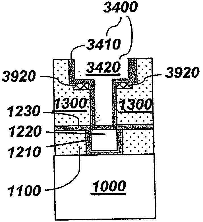
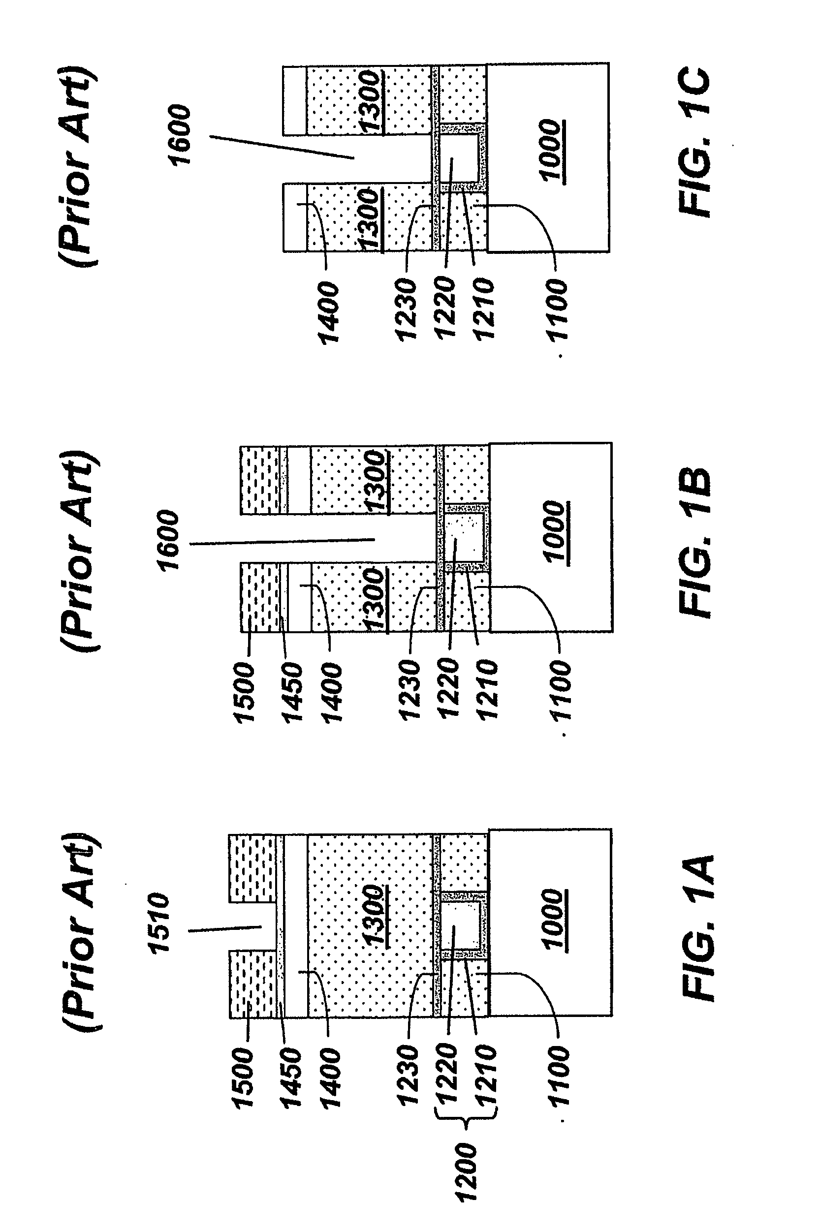
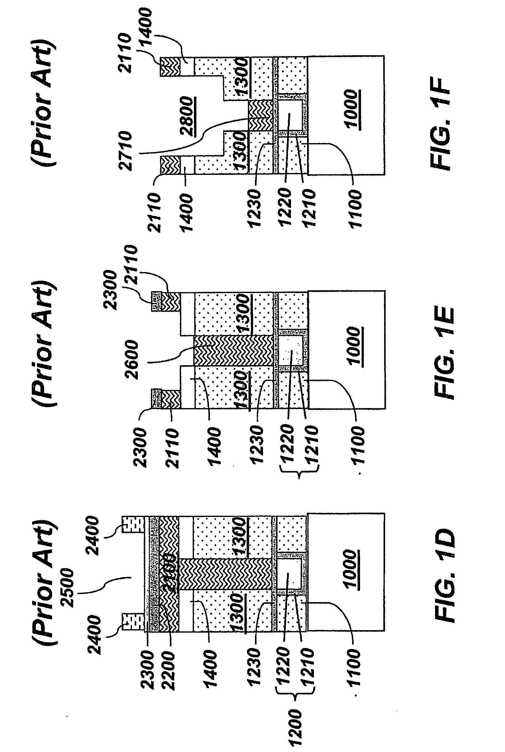
[0101]In embodiment 1, or the first embodiment, of the present invention, the integration sequence including the dual damascene etch and the plasma strip process described in FIGS. 1A-1I and accompanying paragraphs is interrupted after the patterning of the line trench 2800 in the second intermetal dielectric (IMD) layer 1300 and prior to removal of the patterned disposable material layer 2110 and the disposable via fill plug 2710. In other words, the prior art dual damascene process sequence described in FIGS. 1A-1F and accompanying paragraphs above are employed. For the sake of clarity, the prior art metal interconnect structure of FIG. 1F is reproduced as FIG. 2A with the same reference numerals. Thus, the first exemplary metal interconnect structure according to the first embodiment of the present invention shown in FIG. 2A is substantially the same as the prior art structure of FIG. 1F, and may be derived by the same processing steps known in the art.

[...

embodiment 2

Use of a Protective Spacer and Densification of a Trench Bottom Region

[0116]In embodiment 2, or the second embodiment, of the present invention, the integration sequence of the first embodiment is employed up to the step corresponding to fabrication of the metal interconnect structure shown in FIG. 2C. For the sake of clarity, the metal interconnect structure of FIG. 2C is reproduced as FIG. 3A with the same reference numerals. Thus, the second exemplary metal interconnect structure according to the second embodiment of the present invention shown in FIG. 3A is substantially the same as the first exemplary metal interconnect structure of FIG. 2C, and may be derived by the same processing steps disclosed above.

[0117]Referring to FIG. 3B, a near surface region of the second IMD layer 1300 located near the bottom surface of the line trench 2800 is subjected to a densification process that renders the near surface region more robust against damaging effects of plasma in a subsequent pla...


PUM


Abstract

Plasma damage in ultra low k dielectric materials during formation of a dual damascene metal interconnect structure is reduced by providing a protective spacer on sidewalls of a line trench. A densified trench bottom region may be additionally formed directly beneath an exposed horizontal surface of the line trench. The protective spacer and/or the densified trench bottom region protects an ultra low k intermetal dielectric layer from plasma damage during a plasma strip process that is used to remove a disposable via fill plug employed in the dual damascene metal interconnect structure.

Description

RELATED APPLICATIONS[0001]The present application is related to a co-pending U.S. patent application Ser. No. ______ (Attorney Docket No. YOR20070332US1 (21289)), which is incorporated herein by reference.FIELD OF THE INVENTION[0002]The present invention generally relates to methods of manufacturing a semiconductor structure, and particularly, to methods of manufacturing an interconnect structure having reduced signal propagation delay in a semiconductor circuit by minimizing plasma damage to low k and ultra low k organosilicate intermetal dielectric layers with a protective sidewall spacer.BACKGROUND OF THE INVENTION[0003]Advanced semiconductor chips, such as high performance microprocessor, microcontroller and communication chips, require high speed interconnect structures between individual semiconductor devices which are used to perform various functions such as logical operations, storing and retrieving data, providing control signals and the like. With the progress in the semi...

Claims


Application Information

Patent Timeline
IPC IPC(8): H01L23/52H01L21/4763
CPCH01L21/76808H01L21/76814H01L21/76825H01L21/76826H01L21/76831H01L2924/0002H01L23/5329H01L2924/00H01L2221/1063
Inventor ARNOLD, JOHN C.PURUSHOTHAMAN, SAMPATHSANKARAPANDIAN, MUTHUMANICKAMSHOBHA, HOSADURGA K.SPOONER, TERRY A.
Owner GLOBALFOUNDRIES INC
Why Eureka
Try Eureka