System and method for shielding of package on package (PoP) assemblies

a shielding system and shielding technology, applied in the field of radio frequency shielding, can solve the problems of difficult to add a metal shield as a component to the top surface of the substrate, high cost of shielding and low yielding process, and difficult to attach shields on the mother board

Active Publication Date: 2010-12-14
AMKOR TECH SINGAPORE HLDG PTE LTD
View PDF39 Cites 103 Cited by
  • Summary
  • Abstract
  • Description
  • Claims
  • Application Information

AI Technical Summary

Problems solved by technology

However, shield attach on the mother board has several problems.
First, shield attach can be costly and a low yielding process.
In either case, the addition of a metal shield as a component attached to the top surface of the substrate is problematic for several reasons.
First, the addition of a metal shield as a component attached to the top surface of the substrate requires a significant amount of additional space on the package substrate and adds additional thickness to the package.
Second, it can be difficult to transfer mold in and around the

Method used


Image

  • System and method for shielding of package on package (PoP) assemblies
  • System and method for shielding of package on package (PoP) assemblies
  • System and method for shielding of package on package (PoP) assemblies

Examples


Embodiment Construction

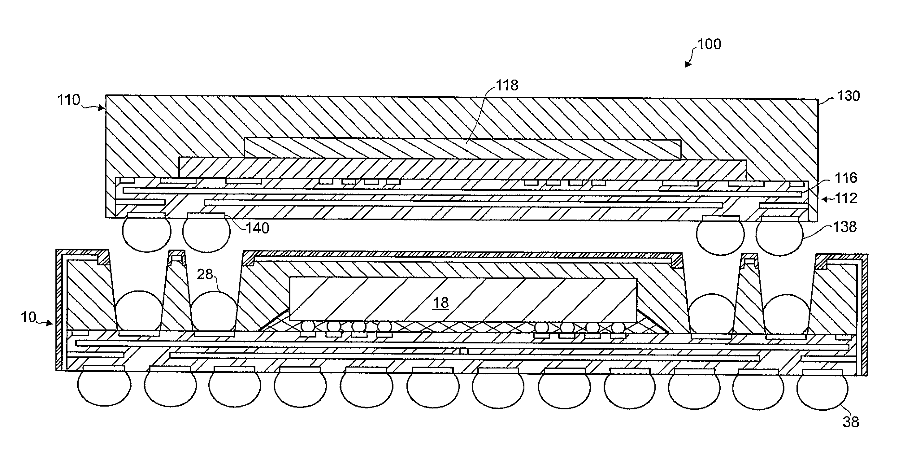
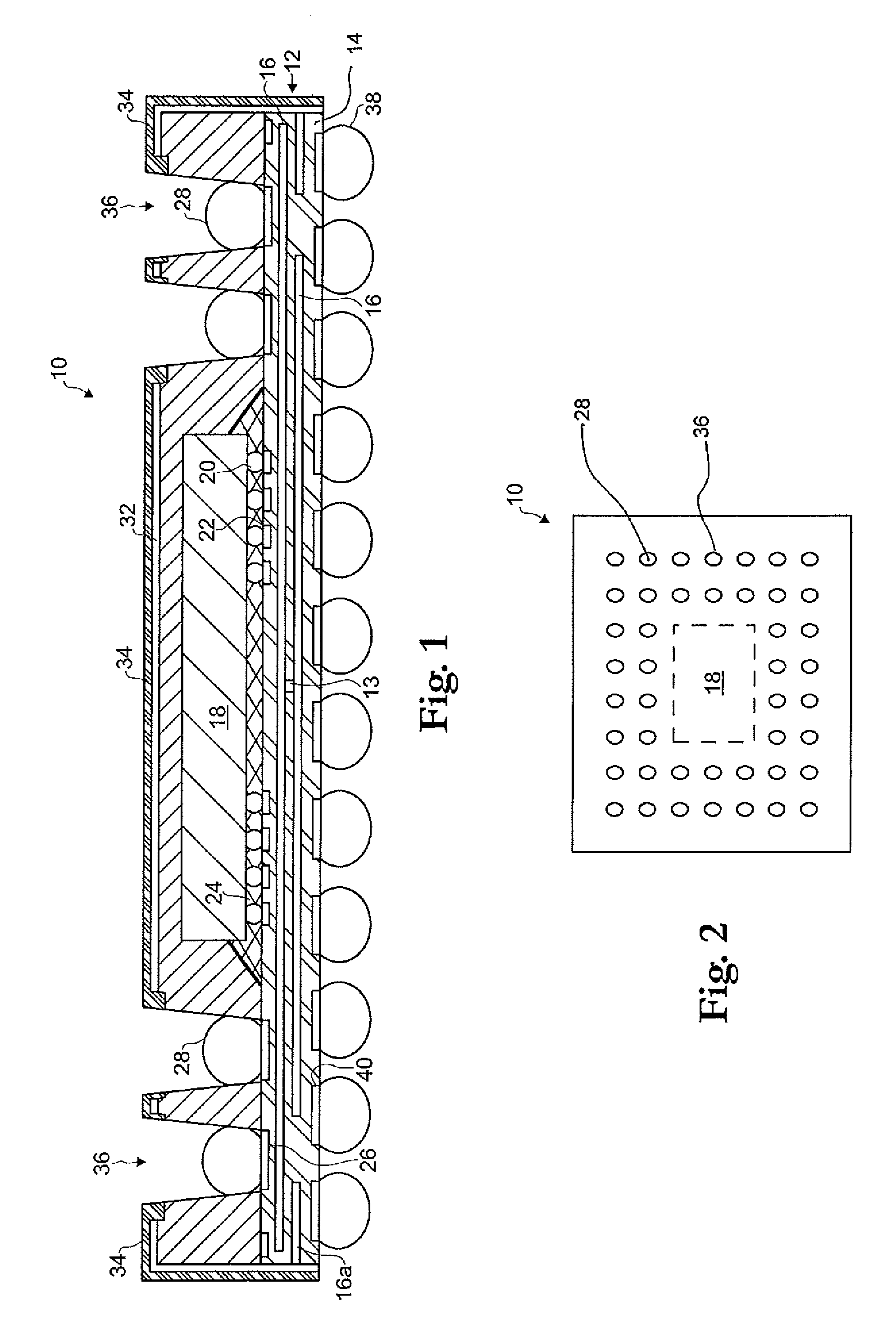
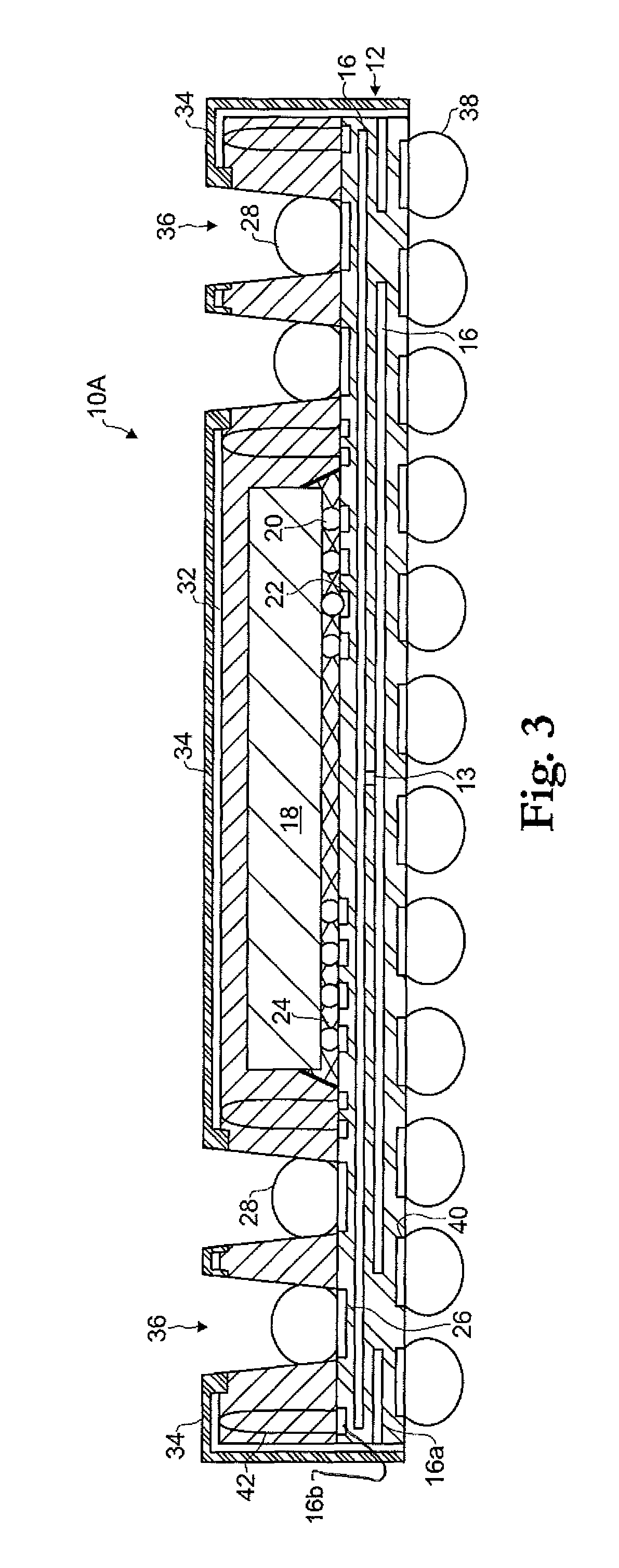
[0016]Referring to FIGS. 1 and 2, a semiconductor package 10 is shown. The semiconductor package 10 is a base package for mounting one or more additional semiconductor packages thereon. The semiconductor package 10 provides an RF shield which leaves land pads exposed and available for mounting an additional semiconductor package while reducing the possibility of shorting the shield material to a solder joint.

[0017]The package 10 has a first substrate 12. The first substrate 12 may be any one chosen from a conventional rigid PCB, a flexible PCB, and an equivalent thereof, but the kind of first substrate 12 is not limited herein. The first substrate 12 includes an insulation layer 14 having predetermined area and thickness. The insulation layer 14 has an approximately planar first surface and an approximately planar second surface opposing the first surface. The first substrate 12 has a plurality of metal traces 16 formed on the first surface of the insulation layer 14. A plurality of...


PUM


Abstract

A semiconductor package has a first substrate having a plurality of metal traces. At least one die is electrically coupled to the first surface of the first substrate. A plurality of land pads is formed on the first surface of the first substrate. A mold compound encapsulates portions of the die and portions of the first surface of the first substrate. A conductive coating is applied to the mold compound and electrically coupled to at least one metal trace. A non-conductive coating is formed over the conductive coating and portions of the mold compound. A plurality of vias is formed through the non-conductive coating and the mold compound to expose the land pads.

Description

FIELD OF THE INVENTION[0001]This invention relates to Radio Frequency (RF) shielding and, more specifically, to a system and method for providing an RF shield for a Package on Package (PoP) base package which leaves contacts of the base package exposed and available for mounting another PoP package on the base package while reducing the possibility of shorting the shield material to a PoP solder joint.BACKGROUND OF THE INVENTION[0002]Radio Frequency (RE) shielding is required on certain semiconductor devices in order to minimize Electro-Magnetic Interference (EMI) radiation from the semiconductor device. RE shielding is further required to prevent RF radiation from external sources from interfering with operation of the semiconductor device.[0003]RF shielding is generally accomplished in one of three ways. A first method is to attach a metal can over the component after the component is attached to the motherboard. However, shield attach on the mother board has several problems. Fir...

Claims


Application Information

Patent Timeline
IPC IPC(8): H01L23/552
CPCH01L23/3128H01L23/552H01L25/105H01L2224/16225H01L2224/73204H01L2924/01078H01L2924/01079H01L2924/15311H01L2924/15331H01L2924/1815H01L2924/3025H01L2224/32225H01L2224/48227H01L2225/06568H01L2225/1023H01L2225/1058H01L2924/00H01L2924/00014H01L2924/00011H01L2224/0401
Inventor SCANLAN, CHRISTOPHER M.
Owner AMKOR TECH SINGAPORE HLDG PTE LTD
Why Eureka
Try Eureka