Semiconductor device having EMI shielding and method therefor

Active Publication Date: 2011-09-06
AMKOR TECH SINGAPORE HLDG PTE LTD
View PDF28 Cites 92 Cited by
  • Summary
  • Abstract
  • Description
  • Claims
  • Application Information

AI Technical Summary

Problems solved by technology

However, shield attach on the mother board has several problems.
First, shield attach can be costly and a low yielding process.
In either case, the addition of a metal shield as a component attached to the top surface of the substrate is problematic for several reasons.
First, the addition of a metal shield as a component attached to the top surface of the substrate requires a significant amount of additional space on the package substrate.
Second, it can be difficult to transfer mold in and around the metal shield to fully encapsulate the semicondu

Method used


Image

  • Semiconductor device having EMI shielding and method therefor
  • Semiconductor device having EMI shielding and method therefor
  • Semiconductor device having EMI shielding and method therefor

Examples


Embodiment Construction

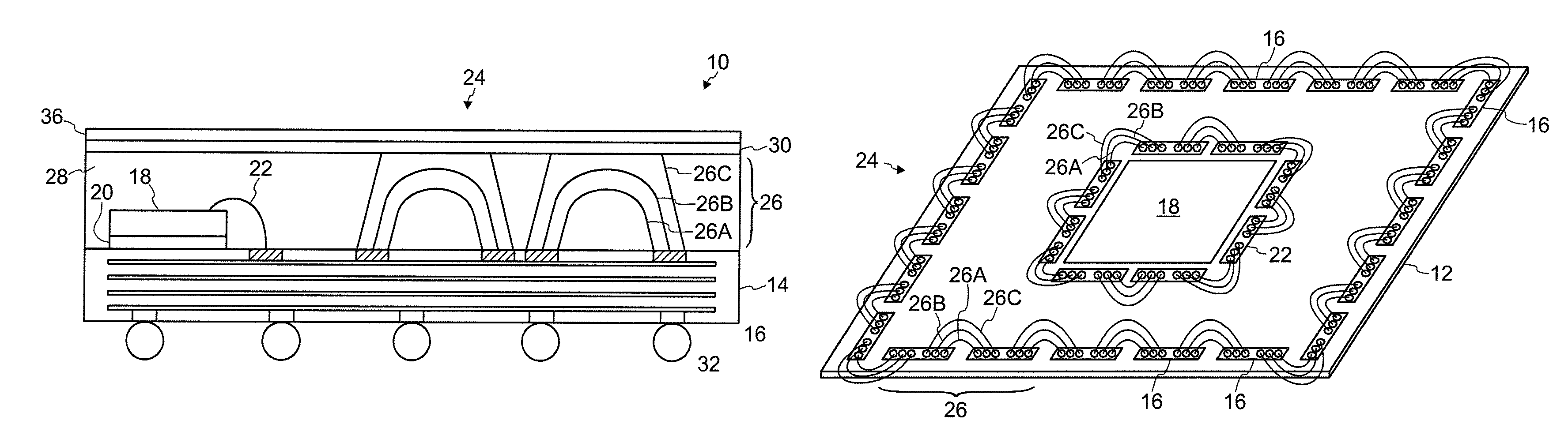
[0021]Referring to FIGS. 1-3, a semiconductor device 10 is shown. The semiconductor device 10 may be a lead type of device, a BGA type of device, a Land Grid Array (LGA) type of device, or the like. The listing of the above should not be seen as to limit the scope of the present invention.

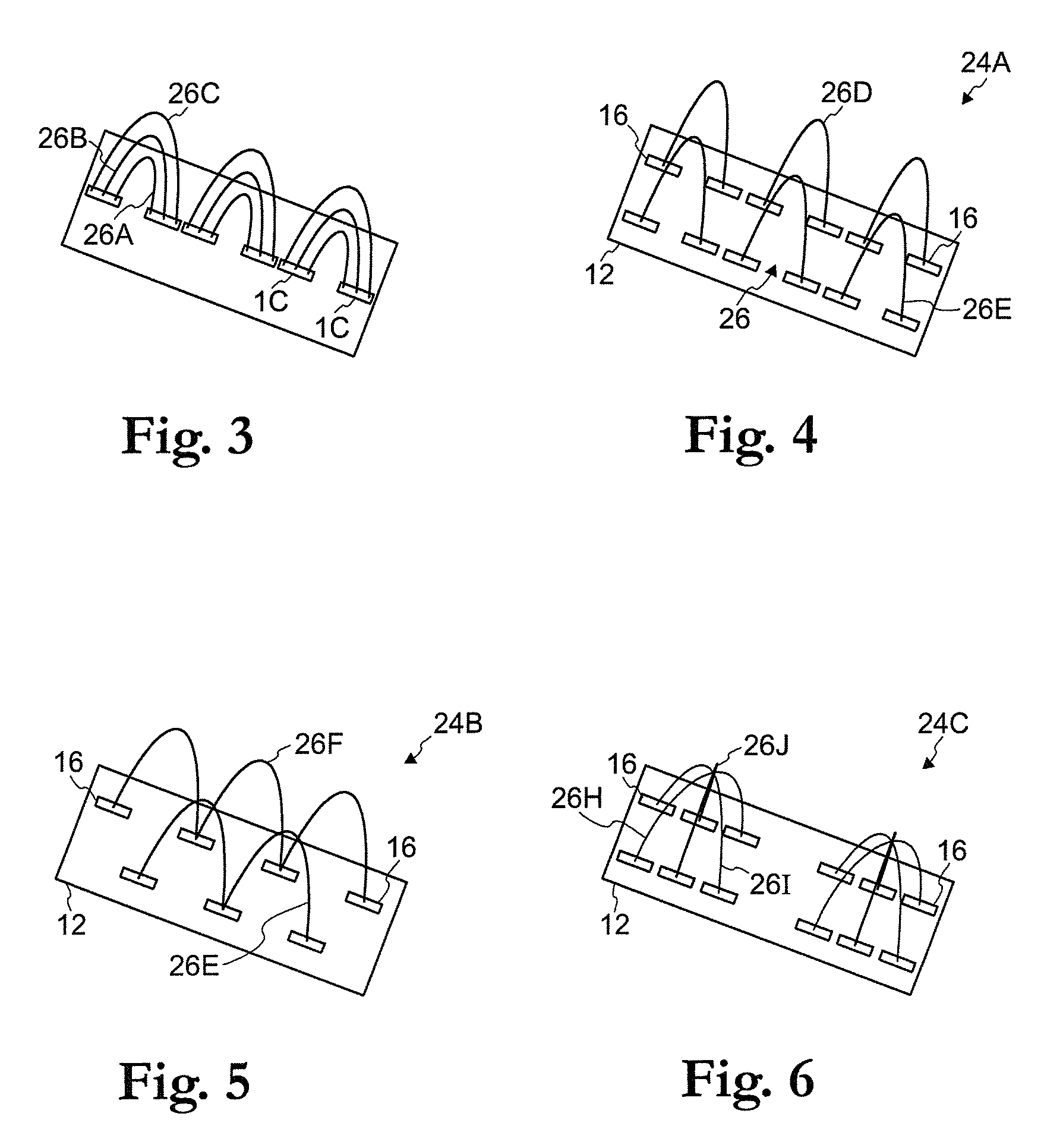
[0022]The device 10 has a substrate 12. The substrate 12 may be any one chosen from a conventional rigid PCB, a flexible PCB, and an equivalent thereof, but the kind of first substrate 12 is not limited herein. The substrate 12 includes an insulation layer 14 having predetermined area and thickness. The insulation layer 14 has an approximately planar first surface and an approximately planar second surface opposing the first surface. The insulation layer 14 will have one or more metal traces 16 formed thereon. In the embodiment shown in FIG. 1, the insulation layer 14 has metal traces 16 formed on the first and second surface of the insulation layer 14. The number of metal traces 16 is not limited ...


PUM


Abstract

A semiconductor device has a substrate having a plurality of metal layers. A die coupled to the substrate. A first wire fence structure is formed on the substrate. A second wire fence structure is formed on the substrate. A mold compound is used for encapsulating the die, a first surface of the substrate, the first wire fence structure, and the second wire fence structure, wherein a top portion of at least one of the first wire fence structure or the second wire fence structure is exposed. A conductive coating is applied to the mold compound and to the portion of the at least one of the first wire fence structure or the second wire fence structure is exposed.

Description

FIELD OF THE INVENTION[0001]This invention relates to semiconductor devices and, more specifically, to a semiconductor device having an integrated Electro-Magnetic Interference (EMI) shielding which is connected to exposed wires coupled to grounding pads.BACKGROUND OF THE INVENTION[0002]Electro-Magnetic Interference (EMI) shielding is required on certain semiconductor devices in order to minimize EMI radiation from the semiconductor device. EMI shielding is further required to prevent EMI radiation from external sources from interfering with operation of the semiconductor device.[0003]EMI shielding is generally accomplished in one of three ways. A first method is to attach a metal can over the component after the component is attached to the motherboard. However, shield attach on the mother board has several problems. First, shield attach can be costly and a low yielding process. External shields soldered to the motherboard further require additional board space.[0004]An alternative...

Claims


Application Information

Patent Timeline
IPC IPC(8): H01L21/44H01L29/40
CPCH01L23/552H01L2224/48247H01L2924/01078H01L2924/01079H01L2924/15311H01L2924/19107H01L2224/48091H01L2924/3025H01L24/48H01L2224/73265H01L2224/48227H01L2224/32225H01L2924/00014H01L2924/00H01L2924/00012H01L2224/451H01L2224/45124H01L2224/45144H01L2224/45147H01L24/45H01L24/73H01L2924/181
Inventor NAVAL, HERBERT DELOS SANTOSSUR, NOEL A.SORIANO, JOHN A.
Owner AMKOR TECH SINGAPORE HLDG PTE LTD
Why Eureka
Try Eureka