Supercharge Your Innovation With Domain-Expert AI Agents!

Resin-sealed semiconductor device, manufacturing method thereof, base material for the semiconductor device, and layered and resin-sealed semiconductor device

a technology of resin-sealed semiconductors and semiconductor devices, which is applied in semiconductor devices, semiconductor/solid-state device details, electrical equipment, etc., can solve the problems of limiting the attempt to achieve higher-speed manufacturing by shortening each wiring, increasing cost and time for development, and intensive progress of forming systems lsi into one chip

Active Publication Date: 2010-12-14
DAI NIPPON PRINTING CO LTD
View PDF13 Cites 2 Cited by
  • Summary
  • Abstract
  • Description
  • Claims
  • Application Information

AI Technical Summary

Benefits of technology

This approach allows for a significantly thinned semiconductor package with improved sealing properties, increased productivity, and enhanced structural stability, facilitating the construction of stacked system packages at a lower cost with increased reliability and workability.

Problems solved by technology

Meanwhile, development of forming a system LSI into one chip has intensively progressed.
However, this approach is based on two-dimensional deployment of wirings, thus limiting an attempt to achieve higher-speed manufacturing by shortening each wiring.
Under present conditions, this approach tends to increase the cost and time for development.
However, the resin-sealed semiconductor device described in this patent document includes a die pad, thus making it difficult to achieve a sufficiently thinned form as currently needed.
However, this system may tend to decrease the degree of freedom in the structure, limiting applicability for a general purpose.Patent Document 1: JP11-307675APatent Document 2: JP11-260989APatent Document 3: JP2002-33434A

Method used


Image

  • Resin-sealed semiconductor device, manufacturing method thereof, base material for the semiconductor device, and layered and resin-sealed semiconductor device
  • Resin-sealed semiconductor device, manufacturing method thereof, base material for the semiconductor device, and layered and resin-sealed semiconductor device
  • Resin-sealed semiconductor device, manufacturing method thereof, base material for the semiconductor device, and layered and resin-sealed semiconductor device

Examples


first embodiment

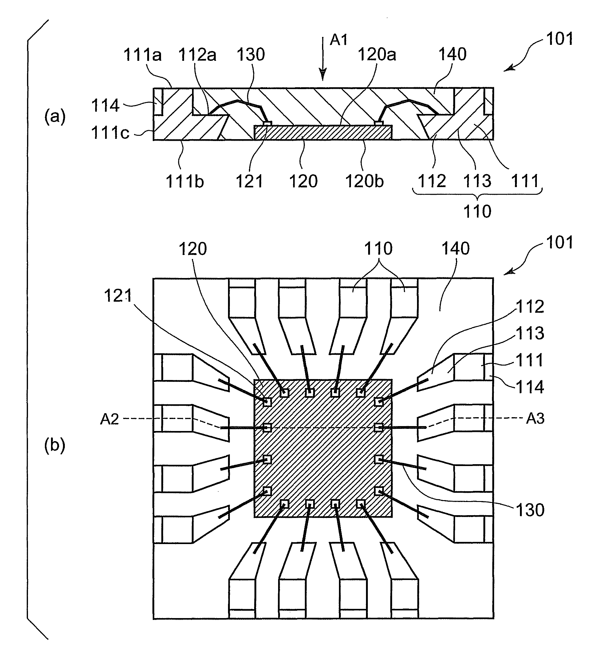
[0090]First of all, the resin-sealed semiconductor device according to the present invention will be described with reference to FIG. 1.

[0091]The resin-sealed semiconductor device 101 includes the semiconductor element 120; a plurality of terminal members 110, each surrounding the semiconductor element and including the external terminal portion 111 connected with an external circuit, the internal terminal portion 112 connected with the semiconductor element 120, and the connecting portion 113 connecting the external terminal portion 111 with the internal terminal portion 112; bonding wires 130, each electrically connecting each terminal 121 of the semiconductor element 120 with the internal terminal portion 112 of each terminal member 110; and the resin sealing portion 140 sealing the semiconductor device 120, terminal members 110 and boding wires 130.

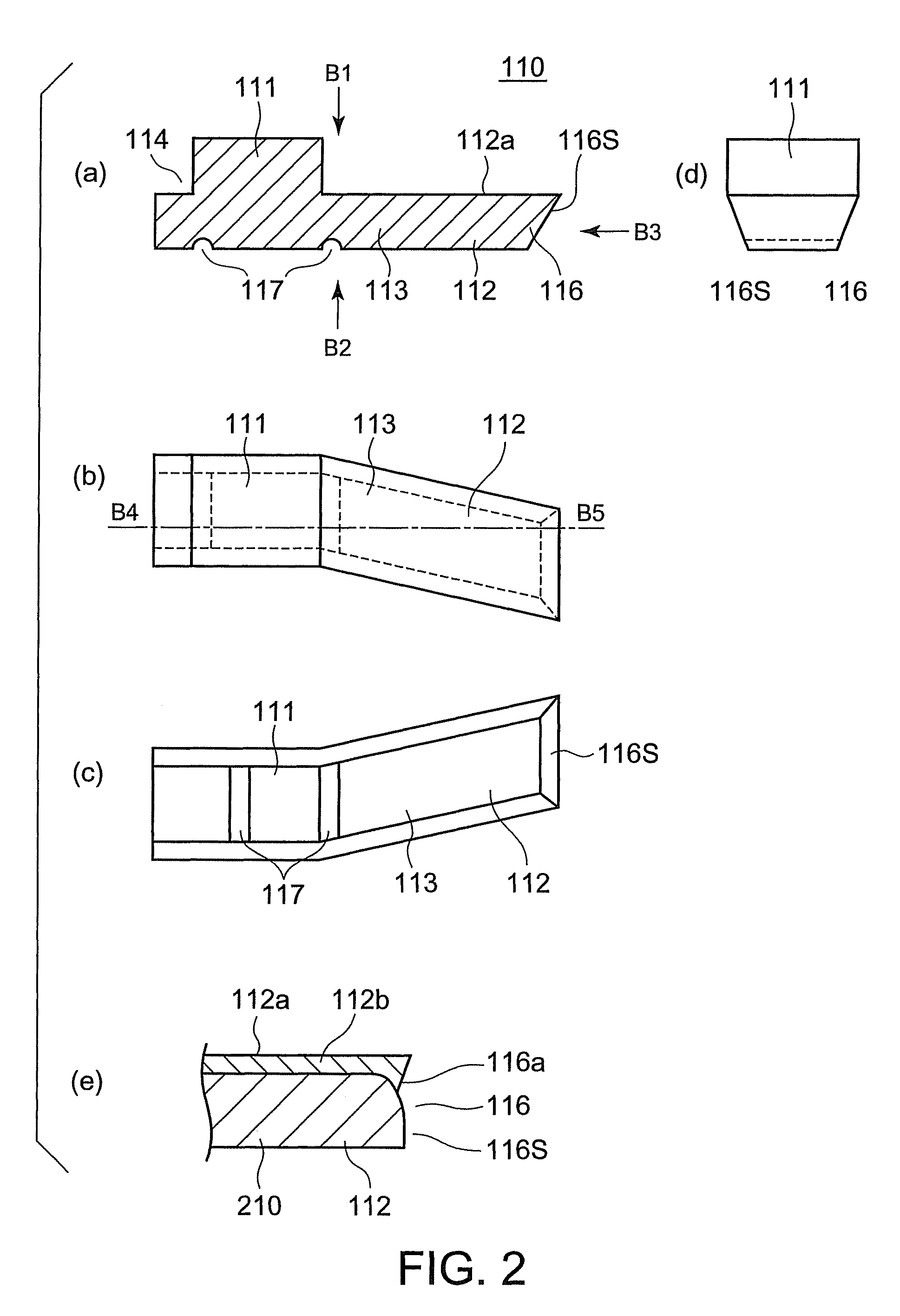
[0092]Each terminal member 110 has a flat rear face 111b and two stepwise front faces 111a, 112a. Each internal terminal portion 112...

second embodiment

[0111]Next, the resin-sealed semiconductor device of the present invention will be described, with reference to FIGS. 3(a) and 3(b).

[0112]The resin-sealed semiconductor device 101 includes the plurality of terminal members 110, semiconductor element 120A having a thickness less than the thickness of each internal terminal portion 112, a predetermined number of terminals 121 provided on the semiconductor element 120A and bonding wires 130 each connecting each terminal 121 with each corresponding internal terminal portion 112. The plurality of terminal members 110 are arranged along peripheral opposite two sides of the semiconductor element 120A. The entire body of the resin-sealed semiconductor device 101 is shaped to fit in the area in which the plurality of terminal members 110 are arranged, and has a thickness not greater than that of the external terminal portion 111 of each terminal member 110. The semiconductor element 120A and bonding wires 130 are sealed by a resin, so as to ...

third embodiment

[0115]Next, the resin-sealed semiconductor device of the present invention will be described, with reference to FIGS. 4(a) and 4(b).

[0116]The resin-sealed semiconductor device 101 includes the plurality of terminal members 110, semiconductor element 120B having a thickness less than the thickness of each internal terminal portion 112, a predetermined number of terminals 121 provided on the semiconductor element 120B and bonding wires 130 each connecting each terminal 121 with each corresponding internal terminal portion 112. The plurality of terminal members 110 are arranged along peripheral opposite two sides of the semiconductor element 120B. The entire body of the resin-sealed semiconductor device 101 is shaped to fit in the area in which the plurality of terminal members 110 are arranged, and has a thickness not greater than that of the external terminal portion 111 of each terminal member 110. The semiconductor element 120B and bonding wires 130 are sealed by a resin, so as to ...


PUM


Abstract

The present invention provides a resin-sealed semiconductor device, which includes a semiconductor element; a plurality of terminal members, each surrounding the semiconductor element and including an external terminal portion, an internal terminal portion and a connecting portion; bonding wires, each connecting the semiconductor element with the internal terminal portion; and a resin-sealing portion sealing the semiconductor element, terminal members and bonding wires. Each terminal member is composed of an inner thinned portion forming the internal terminal portion and an outer thickened portion forming the external terminal portion. A rear face of each internal terminal portion, and a front face, a rear face and an outer side face of each external terminal portion are exposed to the outside from the resin-sealing portion, respectively.

Description

BACKGROUND OF THE INVENTION[0001]1. Field of the Invention[0002]The present invention relates to a small-size and thin-type resin-sealed semiconductor device including terminal members, and a layered and resin-sealed semiconductor device having a structure in which such semiconductor devices are layered.[0003]2. Background Art[0004]In recent years, for miniaturization of the electronic equipment, packaging of a semiconductor part into the electronic equipment with higher density has been required. With such a trend, miniaturization and thinning of the semiconductor part has progressed. Therefore, there is a need for a package including the resin-sealed semiconductor device that can be further thinned at a low cost.[0005]Under such conditions, the resin-sealed semiconductor device, as described in JP11-307675A, having a structure in which both of upper and bottom faces of each connecting lead are exposed, and the resin-sealed semiconductor device, as described in JP11-260989A, having...

Claims


Application Information

Patent Timeline
Patent Type & Authority Patents(United States)
IPC IPC(8): H01L23/48
CPCH01L21/561H01L21/568H01L21/6835H01L23/49548H01L24/06H01L24/85H01L24/97H01L25/105H01L25/50H01L23/3107H01L24/48H01L2224/04042H01L2224/05553H01L2224/05599H01L2224/06136H01L2224/48091H01L2224/48247H01L2224/48465H01L2224/49171H01L2224/85001H01L2224/85399H01L2224/97H01L2924/01028H01L2924/01029H01L2924/01046H01L2924/01047H01L2924/0105H01L2924/01078H01L2924/01079H01L2924/01082H01L2924/014H01L2924/14H01L2924/18165H01L2924/00014H01L2224/85H01L2924/01005H01L2924/01006H01L2924/01033H01L2224/78H01L24/49H01L2924/00H01L2224/45099H01L2225/1029H01L2225/1058H01L2225/1005H01L2224/05554H01L2224/78744H01L2924/181H01L2924/00012H01L23/12H01L23/50H01L25/10H01L25/11
Inventor MASUDA, MASACHIKAIKENAGA, CHIKAOTOMITA, KOJI
Owner DAI NIPPON PRINTING CO LTD
Features
  • R&D
  • Intellectual Property
  • Life Sciences
  • Materials
  • Tech Scout
  • Unparalleled Data Quality
  • Higher Quality Content
  • 60% Fewer Hallucinations
Learn More