Memory system and method using stacked memory device dice, and system using the memory system

a memory system and memory dice technology, applied in the field of memory devices, can solve the problems of slowing the performance of conventional computer systems, exacerbated problems, idle computer systems operating as high-end servers,

Active Publication Date: 2010-12-21
MICRON TECH INC
View PDF27 Cites 107 Cited by
  • Summary
  • Abstract
  • Description
  • Claims
  • Application Information

AI Technical Summary

Problems solved by technology

Yet conventional DRAM devices often do not have the bandwidth to read and write data at these higher speeds, thereby slowing the performance of conventional computer systems.
This problem is exacerbated by the trend toward multi-core processors and multiple processor computer systems.
It is currently estimated that computer systems operating as high-end servers are idle as many as 3 out of every 4 clock cycles because of the limited data bandwidth of system memory devices.
In fact, the limited bandwidth of DRAM devices operating as system memory can reduce the performance of computer systems to as low as 10% of the performance of which they would otherwise be capable.
However, doing so usually requires that write data be serialized and read data deserialized at the memory device interface.
Another approach has been to simply scale up the size of memory devices or conversely shrink their feature sizes, but, for a variety of reasons, scaling has been incapable of keeping up with the geometric increase in the demand for higher data bandwidths.
Proposals have also been made to stack several integrated circuit memory device dice in the same package, but doing so threatens to create a large number of other problems that must be overcome.
One potential problem with stacking memory device dice on top of each other is that it may create signal timing skews between the signals transmitted to or from each of the memory devices.
This can be a considerable problem because there may be a large number of memory device dice in the stack, such as, for example, eight memory devices.
Therefore, it would be very difficult for a memory access device, such as a memory controller or processor, to capture the read data using a single clock signal, particularly as the operating speeds and resulting data transfer rates of memory devices continue to increase.
As the operating speed of memory devices have continued to increase, even this approach has not been sufficient.
However, doing so would require an extensive amount of timing adjustment circuitry in each memory device, thereby reducing the area of each memory device dice available for providing memory capacity.
Furthermore, although the timing problems have been discussed with respect to read data signals, essentially the same type of problems can exist with write data signals, command signals and address signals.
Yet, it is generally considered undesirable to unduly increase the number of terminals in a memory device because of the lack of available area in a memory device package and the large number of conductors that would be required in the bus or circuit board on which the memory device was mounted.

Method used


Image

  • Memory system and method using stacked memory device dice, and system using the memory system
  • Memory system and method using stacked memory device dice, and system using the memory system
  • Memory system and method using stacked memory device dice, and system using the memory system

Examples


Embodiment Construction

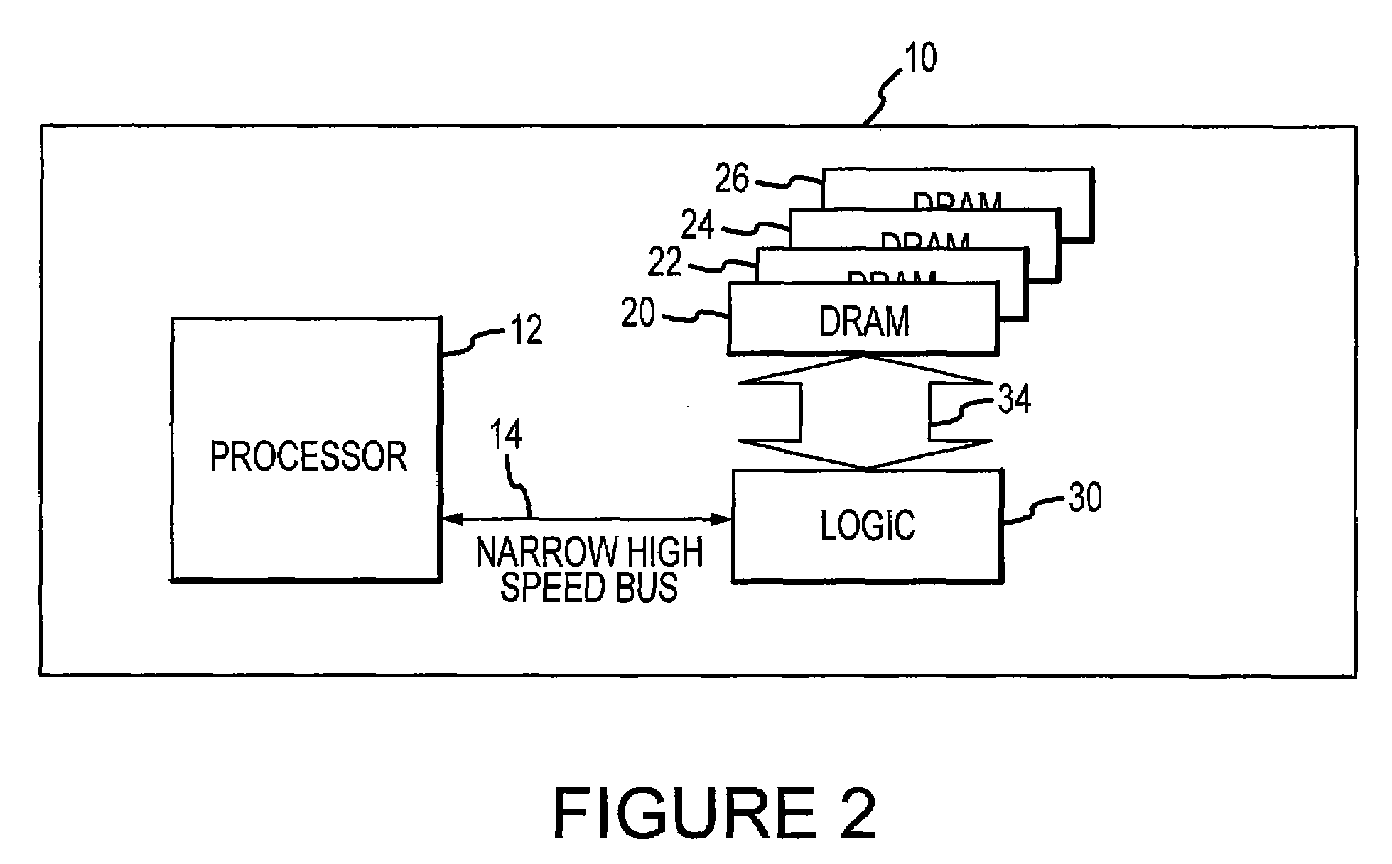
[0015]A computer system including a high-capacity, high bandwidth memory system 10 according to an embodiment of the invention is shown in FIG. 2. The memory system 10 is connected to a processor 12 through a relatively narrow high-speed bus 14 that is divided into downstream lanes and separate upstream lanes (not shown in FIG. 2). The memory system 10 includes 4 DRAM dice 20, 22, 24, 26, which may be identical to each other, stacked on top of each other. Although the memory system 10 includes 4 DRAM dice 20, 22, 24, 26, other embodiments of the memory device use a greater or lesser number of DRAM dice. The stacked DRAM dice 20, 22, 24, 26 are connected to a logic die 30, which serves as the interface with the processor 12. The logic die 30 can be physically positioned relative to DRAM dice 20, 22, 24, 26 in any order, such as by stacking the DRAM dice 20, 22, 24, 26 on top of the logic die 30. However, the logic die 30 could, for example, be positioned in the middle of the stack of...


PUM


Abstract

A memory system and method uses stacked memory device dice coupled to each other and to a logic die. The logic die may include a timing correction system that is operable to control the timing at which the logic die receives signals, such as read data signals, from each of the memory device dice. The timing correction controls the timing of the read data or other signals by adjusting the timing of respective strobe signals, such as read strobe signals, that are applied to each of the memory device dice. The memory device dice may transmit read data to the memory device at a time determined by when it receives the respective strobe signals. The timing of each of the strobe signals is adjusted so that the read data or other signals from all of the memory device dice are received at the same time.

Description

TECHNICAL FIELD[0001]This invention relates to memory devices, and, more particularly, in one or more embodiments to a memory system having a plurality of stacked memory device dice connected to a logic die.BACKGROUND OF THE INVENTION[0002]As memory devices of all types have evolved, continuous strides have been made in improving their performance in a variety of respects. For example, the storage capacity of memory devices has continued to increase at geometric proportions. This increased capacity, coupled with the geometrically higher operating speeds of electronic systems containing memory devices, has made high memory device bandwidth ever more critical. One application in which memory devices, such as dynamic random access memory (“DRAM”) devices, require a higher bandwidth is their use as system memory in computer systems. As the operating speed of processors has increased, processors are able to read and write data at correspondingly higher speeds. Yet conventional DRAM devic...

Claims


Application Information

Patent Timeline
Patent Type & Authority Patents(United States)
IPC IPC(8): G11C8/00
CPCG11C5/02G11C7/1006G11C7/1012G11C7/1051G11C7/1069G11C7/1078G11C7/1096G11C11/4096G11C29/02G11C29/023G11C29/028G06F12/00G11C7/1072G11C7/222G11C11/401G11C2207/107G11C7/10G11C7/22
Inventor LABERGE, PAUL A.JEDDELOH, JOSEPH M.JOHNSON, JAMES B.
Owner MICRON TECH INC
Why Eureka
Try Eureka