Multi-substrate region-based package and method for fabricating the same

a multi-substrate region and package technology, applied in the field of semiconductor packages, can solve the problems of inability to meet the requirement of further increase in i/o connections for electronic products nowadays, limited number of i/o connections provided, and out of date conventional bga package configuration. achieve the effect of improving reliability, good compatibility and increasing yield

Active Publication Date: 2010-12-28
UTAC HEADQUARTERS PTE LTD
View PDF4 Cites 9 Cited by
  • Summary
  • Abstract
  • Description
  • Claims
  • Application Information

AI Technical Summary

Benefits of technology

[0014]Still another objective of the present invention is to provide a multi-substrate region-based package and a method for fabricating the same, which are cost-effective, increase yield and avoid complex packaging.
[0015]A further objective of the present invention is to provide a multi-substrate region-based package and a method for fabricating the same, which provide good compatibility.
[0016]A further objective of the present invention is to provide a multi-substrate region-based package and a method for fabricating the same, which provide a small packaging area, high heat dissipation and good reliability.
[0022]Therefore, the multi-substrate region-based package and the method for fabricating the same in the present invention use the HDP technologies to form a plurality of functional regions on the active surface of the chip. Each of the functional regions has a first electrical connecting portion and a substrate electrically connected the first electrical connecting portion. The integration of the plurality of functional regions in a single chip may increase yield while avoiding the use of the conventional complex SiP packaging technology. In addition, by combining a plurality of substrates with different functional regions of the chip, good compatibility, improved reliability and reduced packaging area can be provided. Moreover, the non-active surface of the chip is exposed, such that heat dissipation of the package can be greatly enhanced.
[0023]Furthermore, in the present invention, the chip is divided into a plurality of functional regions each being mounted with a corresponding substrate, such that system integration and circuitry design can be performed on each of the functional regions respectively, thereby allowing the package to be designed or made smaller and thinner as desired. This arrangement can also prevent bonding wires from being torn or pulled on each of the functional regions when the functional region is subjected to thermal expansion, thereby maintaining integrity of the bonding wires.

Problems solved by technology

Such conventional leadframe-based semiconductor package however has a drawback that the leads serving as input / output (I / O) connections can only be disposed around the encapsulant, that is, the number of I / O connections provided is limited by the size of the encapsulant, thereby failing to fulfill the requirement of further increase in I / O connections for the electronic products nowadays.
However, the conventional BGA package configuration has gone out of date due to its poor compatibility with the progress trends of having lower profile, more functions and shorter life span for the electronic products.

Method used


Image

  • Multi-substrate region-based package and method for fabricating the same
  • Multi-substrate region-based package and method for fabricating the same
  • Multi-substrate region-based package and method for fabricating the same

Examples


first embodiment

[0029]FIGS. 2A to 2G are schematic diagrams showing a multi-substrate region-based package and a method for fabricating the same according to a first embodiment of the present invention.

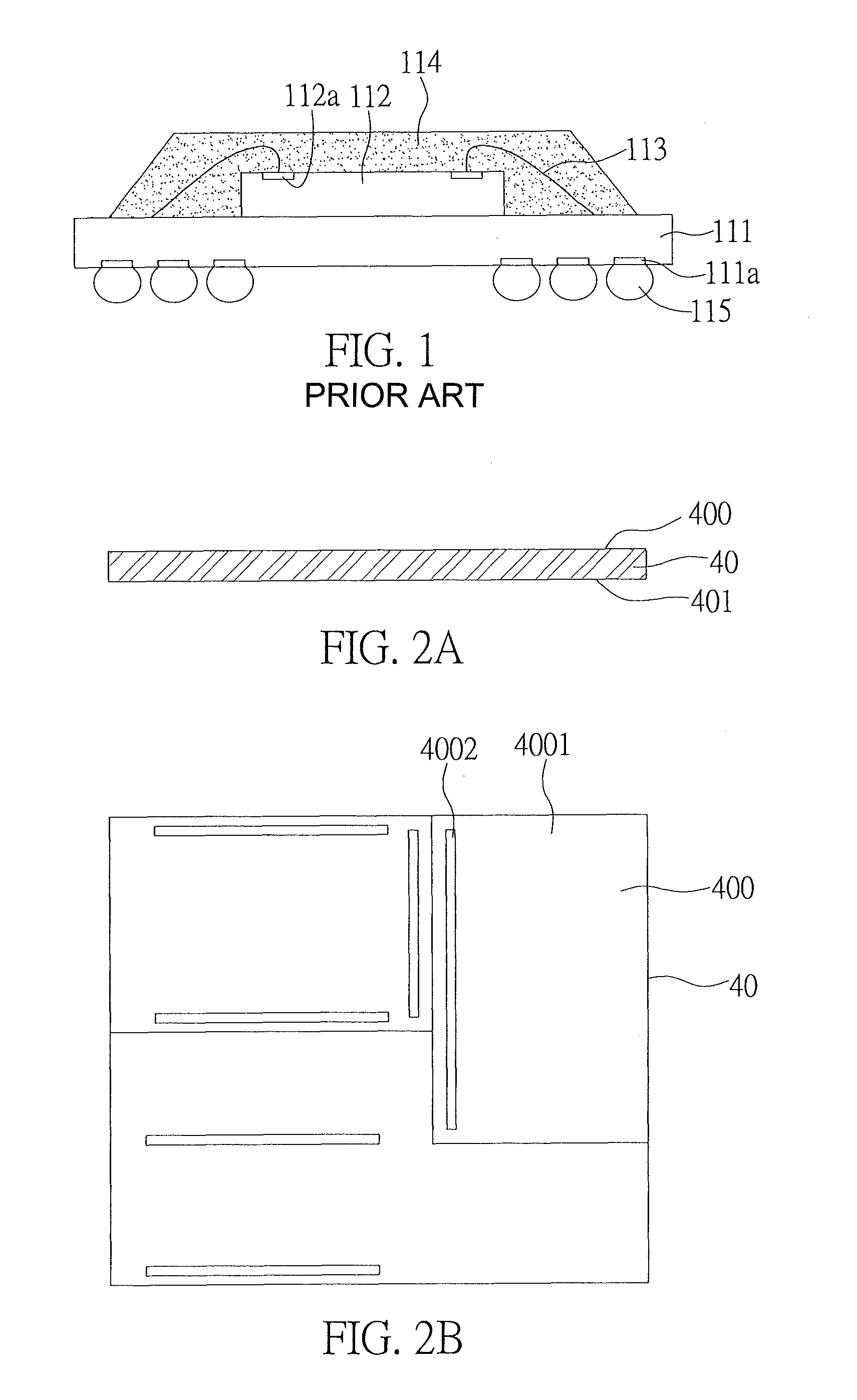
[0030]As shown in FIGS. 2A and 2B, a chip 40 having an active surface 400 and a non-active surface 401 is provided. The active surface 400 of the chip 40 is divided into a plurality of functional regions 4001 each having an independent first electrical connecting portion 4002. The first electrical connecting portion 4002 can be situated on one side, two opposite sides or three sides of the functional region 4001. If there is sufficient room, the first electrical connecting portion 4002 may also be situated on four sides of the functional region 4001.

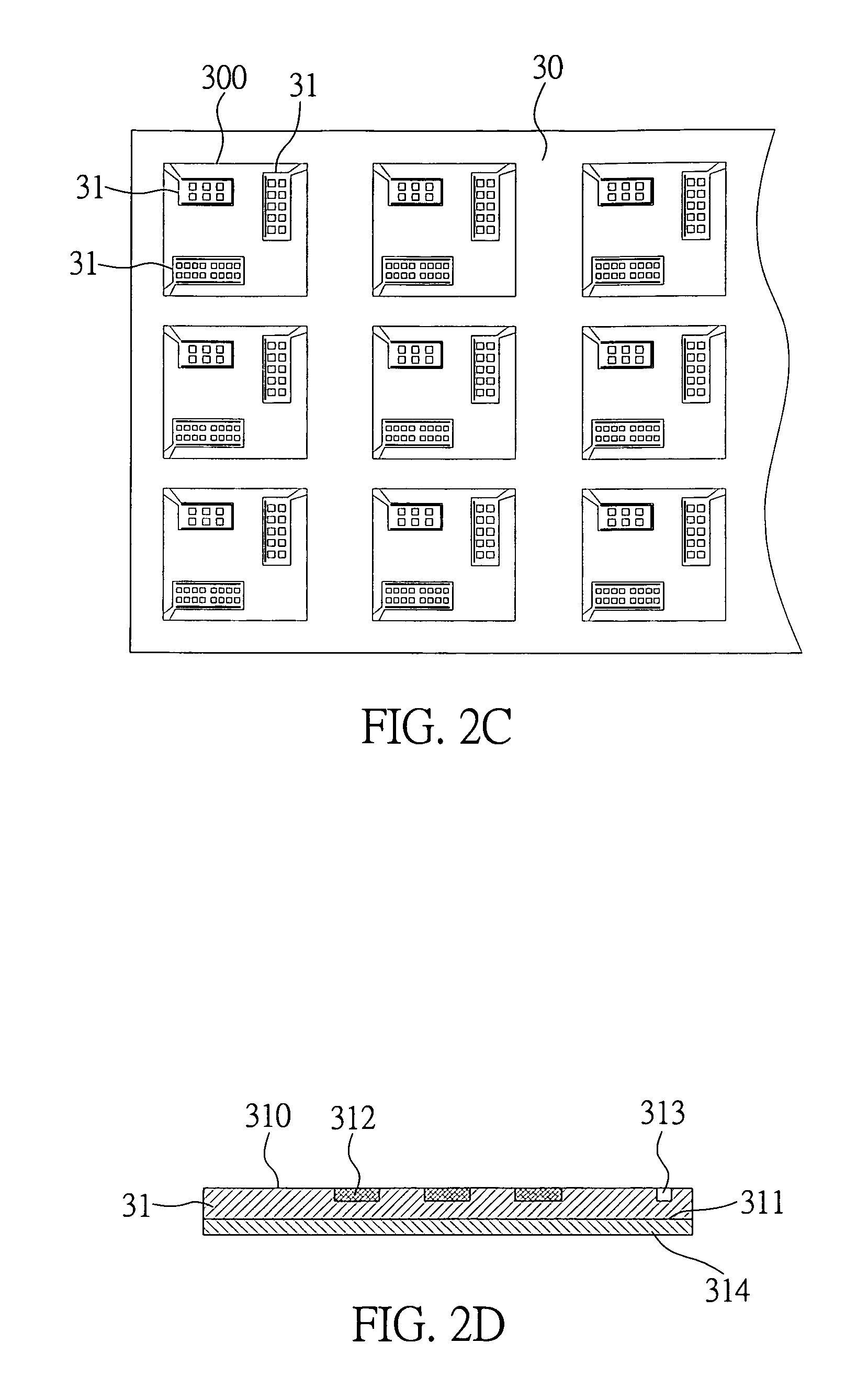
[0031]As shown in FIG. 2C, a substrate strip 30 is provided. The substrate strip 30 is formed with a plurality of openings 300, with a plurality of substrates 31 being disposed in the openings 300 respectively and connected to the substrate strip 30. Refe...

second embodiment

[0039]FIGS. 3A to 3C are schematic diagrams showing a multi-substrate region-based package and a method for fabricating the same according to a second embodiment of the present invention. The second embodiment differs from the above first embodiment in that in the second embodiment, a plurality of stacked chips are disposed in the package.

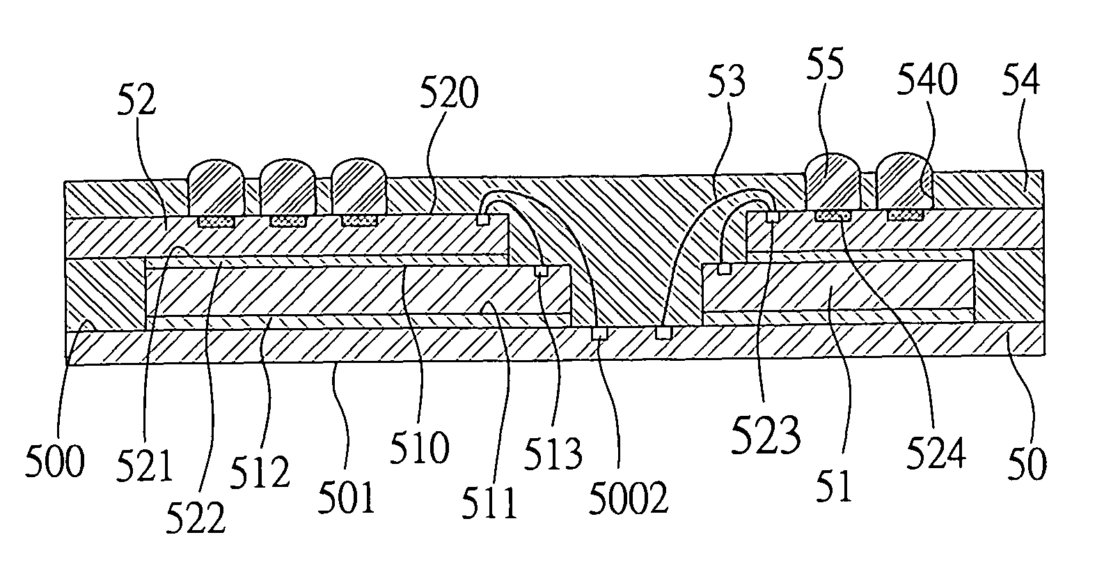
[0040]As shown in FIG. 3A, a chip 50 having an active surface 500 and a non-active surface 501 (referring also to FIG. 3B) is provided. The active surface 500 of the chip 50 is divided into a plurality of functional regions 5001 each having an independent first electrical connecting portion 5002.

[0041]As shown in FIG. 3B, a plurality of sub-chips 51 are provided, each of the sub-chips 51 having an active surface 510 and a non-active surface 511. The active surface 510 of the sub-chip 51 is formed with a third electrical connecting portion 513, and the non-active surface 511 of the sub-chip 51 has an adhesive layer 512 attached thereto, allowing the...

third embodiment

[0045]FIG. 4 is a schematic diagram showing a multi-substrate region-based package according to a third embodiment of the present invention. In the above first and second embodiments, the substrate is smaller in area that that of the corresponding functional region of the chip, while in this third embodiment, the substrate can be larger in size than that of the functional region of the chip.

[0046]As shown in FIG. 4, each of the substrates 61 is larger in area than that of a corresponding one of the functional regions 6000 of the active surface 600 of the chip 60. The second electrical connecting portion 6101 of the ball mounting surface 610 of each of the substrates 61 is electrically connected to the first electrical connecting portion 6001 of the corresponding functional region 6000 of the chip 60, and a conductive material is disposed on the bond pads of each of the substrates 61. The rest of the fabrication processes and structural arrangement are substantially identical to thos...


PUM


Abstract

A multi-substrate region-based package and a method for fabricating the same are provided. An active surface of a chip is divided into a plurality of functional regions, and each of the functional regions is electrically connected to a corresponding substrate via bonding wires. Each of the functional regions has a separate system, and the circuit layout thereof is not limited by the substrate or other systems but can be flexibly and independently designed, thereby allowing the package to be made smaller and thinner. Each set of the functional region and its corresponding substrate functions as an independent unit, such that the substrates are not affected by each other, thereby providing good compatibility, improved reliability and reduced packaging area.

Description

BACKGROUND OF THE INVENTION[0001]1. Field of the Invention[0002]The present invention relates to semiconductor packages, and more particularly, to a multi-substrate region-based package and a method for fabricating the same.[0003]2. Description of Related Art[0004]Conventional leadframe-based semiconductor package, such as a quad flat package (QFP), is fabricated by preparing a leadframe comprising a die pad and a plurality of leads, mounting a chip on the die pad, forming a plurality of bonding wires for electrically connecting bond pads formed on the chip to the corresponding leads, and encapsulating the chip and the bonding wires by an encapsulant.[0005]Such conventional leadframe-based semiconductor package however has a drawback that the leads serving as input / output (I / O) connections can only be disposed around the encapsulant, that is, the number of I / O connections provided is limited by the size of the encapsulant, thereby failing to fulfill the requirement of further increa...

Claims


Application Information

Patent Timeline
Patent Type & Authority Patents(United States)
IPC IPC(8): H01L23/48
CPCH01L23/49833H01L24/32H01L24/33H01L24/49H01L24/73H01L24/83H01L24/91H01L24/97H01L25/0652H01L25/50H01L23/3157H01L23/49816H01L24/29H01L24/48H01L2224/32014H01L2224/48091H01L2224/48227H01L2224/4824H01L2224/49H01L2224/73215H01L2224/73265H01L2224/838H01L2224/97H01L2924/01004H01L2924/01082H01L2924/078H01L2924/14H01L2924/15311H01L2224/32225H01L2924/01006H01L2924/01033H01L2924/01076H01L2924/014H01L2224/32145H01L2924/18165H01L2224/06135H01L2224/06136H01L2224/83H01L2224/85H01L2924/00014H01L2924/00H01L2924/00012H01L2924/181H01L2224/45099H01L2224/05599H01L23/12H01L23/48
Inventor TSAI, SHIANN-TSONG
Owner UTAC HEADQUARTERS PTE LTD
Why Eureka
Try Eureka