Manufacturing method of semiconductor device

a manufacturing method and technology for semiconductor devices, applied in the direction of semiconductor devices, basic electric elements, electrical equipment, etc., can solve the problems of increasing leakage current of misfet, and achieve the effect of reducing leakage current, increasing misfet leakage current, and increasing thickness of gate insulating films

Inactive Publication Date: 2011-01-04
RENESAS ELECTRONICS CORP
View PDF8 Cites 5 Cited by
  • Summary
  • Abstract
  • Description
  • Claims
  • Application Information

AI Technical Summary

Benefits of technology

[0007]In recent years, however, with the trend of scaling down the size of MISFET constituting a semiconductor device, the thickness of a gate insulating film has been rapidly reduced. When the thickness of a gate insulating film is reduced, a phenomenon in which electrons pass through the gate insulating film occurs due to the tunnel effect. By this phenomenon, tunnel current flows in the gate insulating film. As a result, the leakage current of the MISFET increases.
[0008]Therefore, studies on the replacement of a silicon oxide film used as a gate insulating film with a high-dielectric-constant film with a dielectric constant higher than that of a silicon oxide film have been proceeding. This is because, when a high-dielectric-constant film is used to form a gate insulating film, even if the capacitance is the same as that of the case of using a silicon oxide film, the actual physical thickness can be increased by a factor of “dielectric constant of high-dielectric-constant film / dielectric constant of silicon oxide film”, and as a result, the leakage current can be reduced. As a material of a high-dielectric-constant film, metal oxides such as hafnium (Hf) oxide and zirconium (Zr) oxide have been studied.
[0013]Therefore, the studies have been made on the formation of the gate electrode disposed on the gate insulating film from a metal film instead of a polysilicon film in the case where a high-dielectric-constant film with a dielectric constant higher than that of a silicon oxide film is used for a gate insulating film. If a metal film is used to form the gate electrode, the threshold voltage can be adjusted by selecting the type of the metal film instead of adjusting the threshold voltage by implanting an impurity like in the case of using the polysilicon film. Therefore, it is possible to solve the problem of the above-described Fermi level pinning by using a metal film for a gate electrode. Furthermore, since no polysilicon film is used for the gate electrode, the problem of the depletion of the gate electrode can also be solved.
[0021]An object of the present invention is to provide a technology capable of improving the reliability of a semiconductor device without unnecessarily exposing a semiconductor substrate in the manufacturing technology of a semiconductor device in which a high-dielectric-constant film having a dielectric constant higher than that of a silicon oxide film is used for a gate insulating film and different high-dielectric-constant films are used to form a gate insulating film of an n-channel MISFET and a gate insulating film of a p-channel MISFET.
[0028]According to the representative embodiment, the reliability of a semiconductor device can be improved without unnecessarily exposing a semiconductor substrate in the manufacturing technology of a semiconductor device in which a high-dielectric-constant film having a dielectric constant higher than that of a silicon oxide film is used for a gate insulating film and different high-dielectric-constant films are used to form a gate insulating film of an n-channel MISFET and a gate insulating film of a p-channel MISFET.

Problems solved by technology

As a result, the leakage current of the MISFET increases.
As described above, the leakage current passing through the gate insulating film can be reduced by using a high-dielectric-constant film as a gate insulating film of a MISFET, but it causes new problems.

Method used


Image

  • Manufacturing method of semiconductor device
  • Manufacturing method of semiconductor device
  • Manufacturing method of semiconductor device

Examples


first embodiment

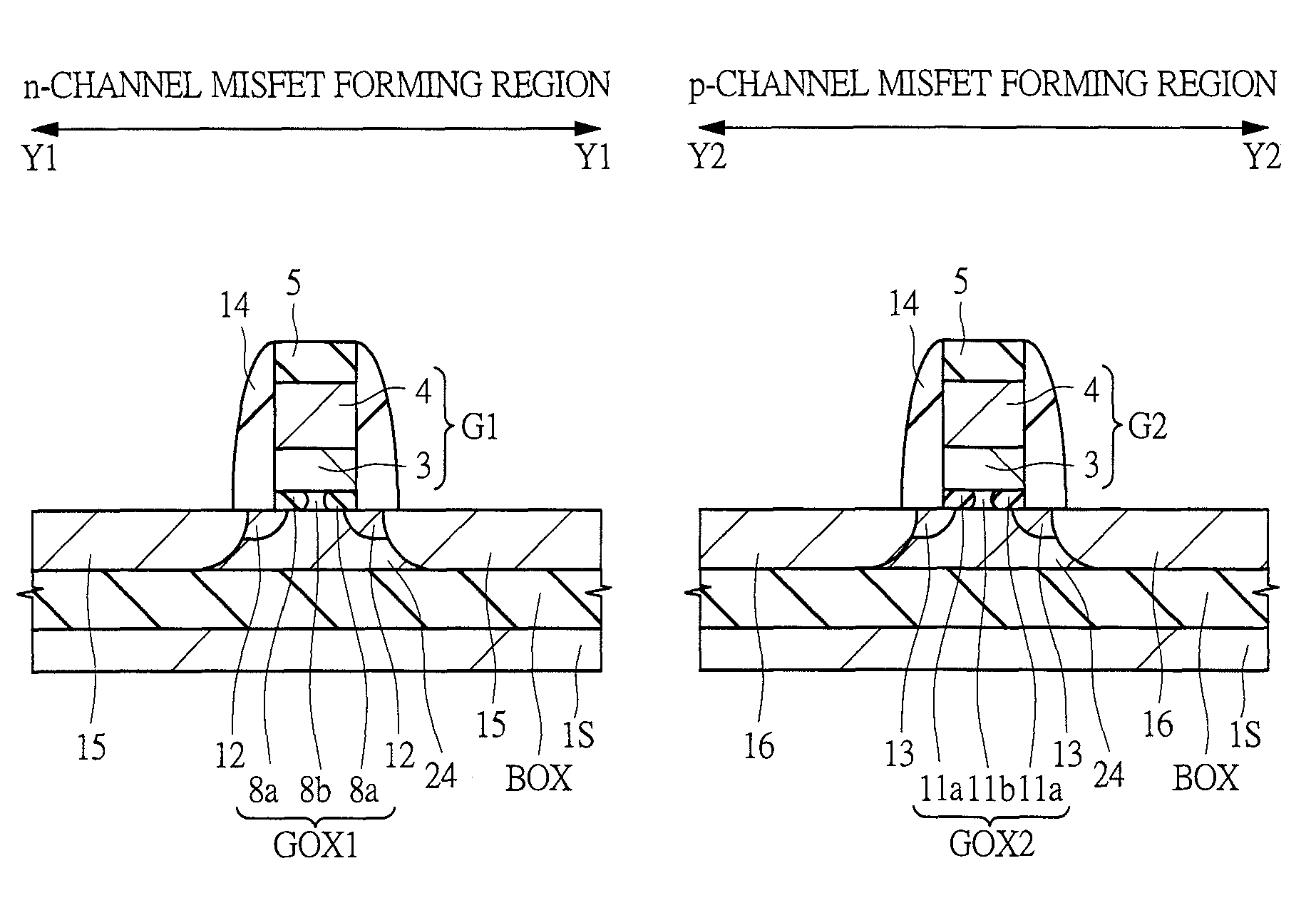
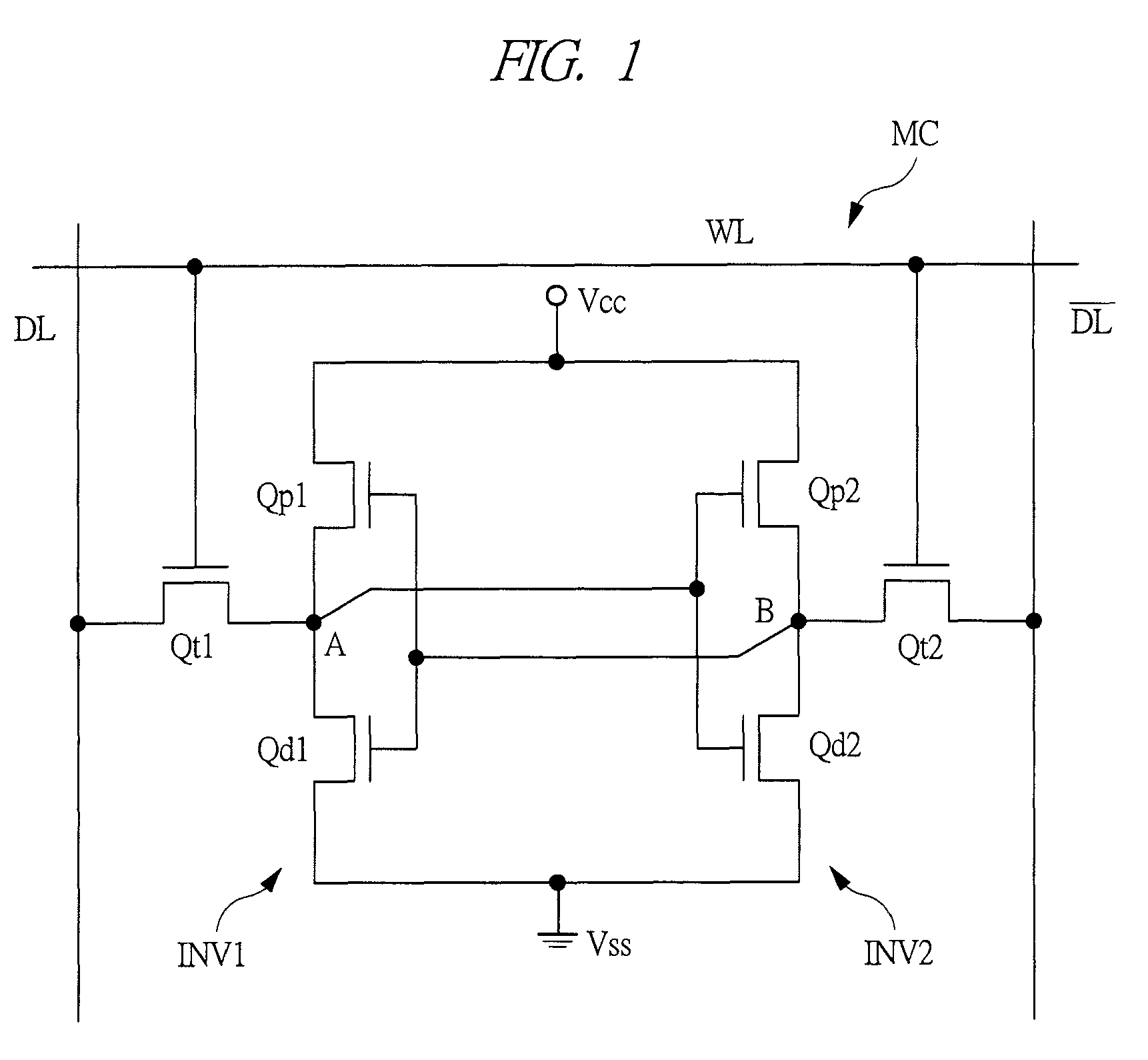
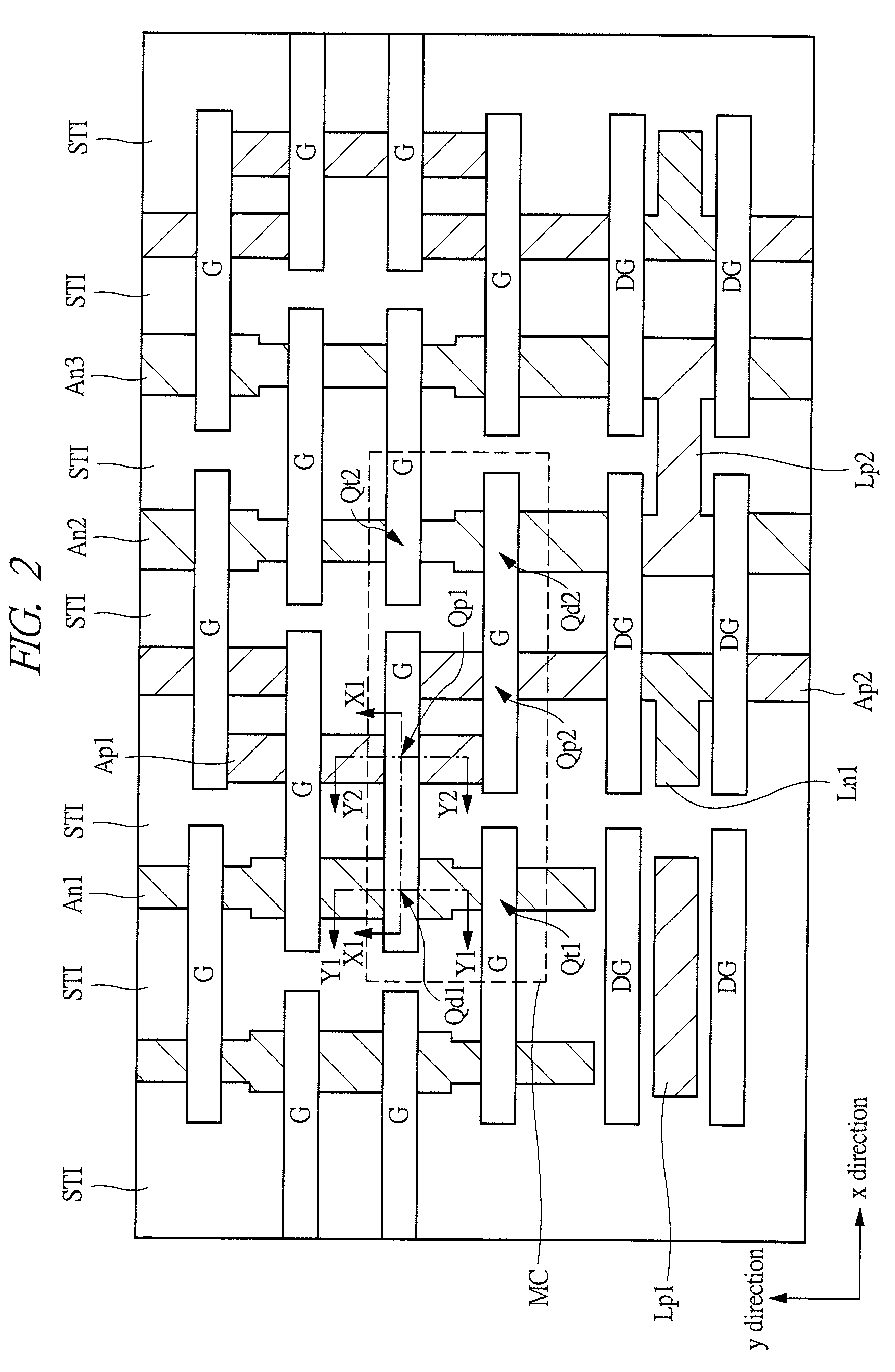
[0086]The first embodiment will be described with an SRAM (Static Random Access Memory) being taken as an example of a semiconductor device. First, an equivalent circuit of a memory cell MC constituting an SRAM will be described. FIG. 1 is an equivalent circuit diagram showing the memory cell MC of the SRAM according to the first embodiment. As shown in FIG. 1, this memory cell is disposed at an intersection between a pair of complementary data lines (data line DL and data line / DL) and a word line WL, and is constituted of a pair of driver MISFETs Qd1 and Qd2, a pair of load MISFETs Qp1 and Qp2, and a pair of transfer MISFETs Qt1 and Qt2. The n-channel MISFETs are used for the driver MISFETs Qd1 and Qd2 and the transfer MISFETs Qt1 and Qt2, and the p-channel MISFETs are used for the load MISFETs Qp1 and Qp2.

[0087]Of the six MISFETs constituting the memory cell MC, the driver MISFET Qd1 and the load MISFET Qp1 form a CMOS inverter INV1, and the driver MISFET Qd2 and the load MISFET ...

second embodiment

[0166]In the second embodiment, the example where the diffusion of an element by an element supply film is performed after forming an offset spacer on a sidewall of a gate electrode will be described. Since the manufacturing method of a semiconductor device according to the second embodiment is almost the same as the manufacturing method of a semiconductor device according to the first embodiment, the description will be made while placing an emphasis on the difference therebetween.

[0167]The process from FIG. 12 to FIG. 15 is the same as that of the first embodiment. Subsequently, as shown in FIG. 31, a silicon nitride film is formed on the whole surface of the semiconductor substrate 1S. Then, the silicon nitride film is anisotropically etched to form offset spacers 20 on the sidewalls of the gate electrode G1 (including the silicon nitride film 5 to be the cap insulating film) and the sidewalls of the gate electrode G2 (including the silicon nitride film 5 to be the cap insulating...

third embodiment

[0175]In the third embodiment, the example where the first insulating film exposed on the semiconductor substrate 1S is removed after forming a gate electrode and a silicon oxide film is formed in the region where the semiconductor substrate 1S is exposed, and thereafter, an element is diffused from an element supply film into the first insulating film will be described. Since the manufacturing method of a semiconductor device according to the third embodiment is almost the same as the manufacturing method of a semiconductor device according to the first embodiment, the description will be made while placing an emphasis on the difference therebetween.

[0176]The process from FIG. 12 to FIG. 15 is the same as that of the first embodiment. Next, as shown in FIG. 34, the exposed first insulating film 2 is removed. By this means, the first insulating film 2 is formed only just below the gate electrode G1 and the gate electrode G2. Although the surface of the semiconductor substrate 1S is ...


PUM


Abstract

After forming a first gate electrode and a second gate electrode on a semiconductor substrate, a silicon oxide film is formed to cover an n-channel MISFET forming region, and a p-channel MISFET forming region is exposed. Subsequently, after a first element supply film made of, for example, an aluminum oxide film is formed on the whole surface of the semiconductor substrate, a heat treatment is performed. By this means, a high-concentration HfAlO film and a low-concentration HfAlO film are formed by diffusing aluminum into the first insulating film just below the second gate electrode. Thereafter, by using a magnesium oxide film as a second element supply film, magnesium is diffused into the first insulating film just below the first gate electrode, thereby forming a high-concentration HfMgO film and a low-concentration HfMgO film.

Description

CROSS-REFERENCE TO RELATED APPLICATION[0001]The present application claims priority from Japanese Patent Application No. JP 2008-135703 filed on May 23, 2008, the content of which is hereby incorporated by reference into this application.TECHNICAL FIELD OF THE INVENTION[0002]The present invention relates to a technology for manufacturing a semiconductor device, and more particularly to a technology effectively applied to the manufacture of a semiconductor device including a MISFET (Metal Insulator Semiconductor Field Effect Transistor) in which a high-dielectric-constant film having a dielectric constant higher than that of a silicon oxide film is used as a gate insulating film.BACKGROUND OF THE INVENTION[0003]Japanese Patent Application Laid-Open Publication No. 2003-249649 (Patent Document 1) describes a technology for suppressing the formation of interface oxide layers on and below a gate insulating film while using a high-dielectric-constant material as the gate insulating film....

Claims


Application Information

Patent Timeline
Patent Type & Authority Patents(United States)
IPC IPC(8): H01L21/8238
CPCH01L21/28167H01L21/823842H01L21/823857H01L29/512H01L29/517H01L29/7833
Inventor MISE, NOBUYUKIMOROOKA, TETSU
Owner RENESAS ELECTRONICS CORP
Why Eureka
Try Eureka