Substrate processing apparatus and method

a technology for processing apparatus and substrates, applied in chemical apparatus and processes, spraying apparatus, crystal growth process, etc., can solve the problems of unnecessarily high temperature of radiation target objects, increased cost, and tendency of electron beams radiated onto films to damage films, etc., to prevent an increase in cost and control the temperature of substrates stably

Inactive Publication Date: 2011-01-11
TOKYO ELECTRON LTD
View PDF6 Cites 131 Cited by
  • Summary
  • Abstract
  • Description
  • Claims
  • Application Information

AI Technical Summary

Benefits of technology

[0012]An object of the present invention is to provide a substrate processing apparatus and method for curing a target film formed on the target surface of a substrate while radiating UV rays (ultraviolet rays) onto the target film, wherein the apparatus and method can prevent an increase in cost and can stably control the temperature of the substrate.
[0014]According to a second aspect of the present invention, there is provided a substrate processing method for radiating UV rays (ultraviolet rays) onto a target film formed on a target surface of a substrate to perform a curing process of the target film, the substrate processing method comprising: placing the substrate on a plurality of support pins disposed on a hot plate; then, heating the substrate to a predetermined temperature by the hot plate; and then, radiating UV rays onto the target surface of the substrate supported on the support pins, thereby performing the curing process, wherein the support pins are preset to provide a predetermined thermal conductivity, and the hot plate is preset to have a predetermined thermal capacity, and wherein the curing process comprises conducting heat, applied to the substrate by the UV rays, through the support pins to the hot plate, and absorbing the heat conducted through the support pins into the hot plate, thereby preventing the substrate from being overheated.

Problems solved by technology

The EB curing process entails a problem in curing an insulating film having a low specific dielectric constant (k-value) (which may be referred to as “Low-k film”), such that an electron beam radiated onto the film tends to damage the film.
Consequently, another problem may arise such that the temperature of the radiation target object becomes unnecessarily higher.
Further, in order to control the temperature increase of the radiation target object, a cooling function needs to be added, so the apparatus becomes more complex and thereby brings about an increase in cost.

Method used


Image

  • Substrate processing apparatus and method
  • Substrate processing apparatus and method
  • Substrate processing apparatus and method

Examples


Embodiment Construction

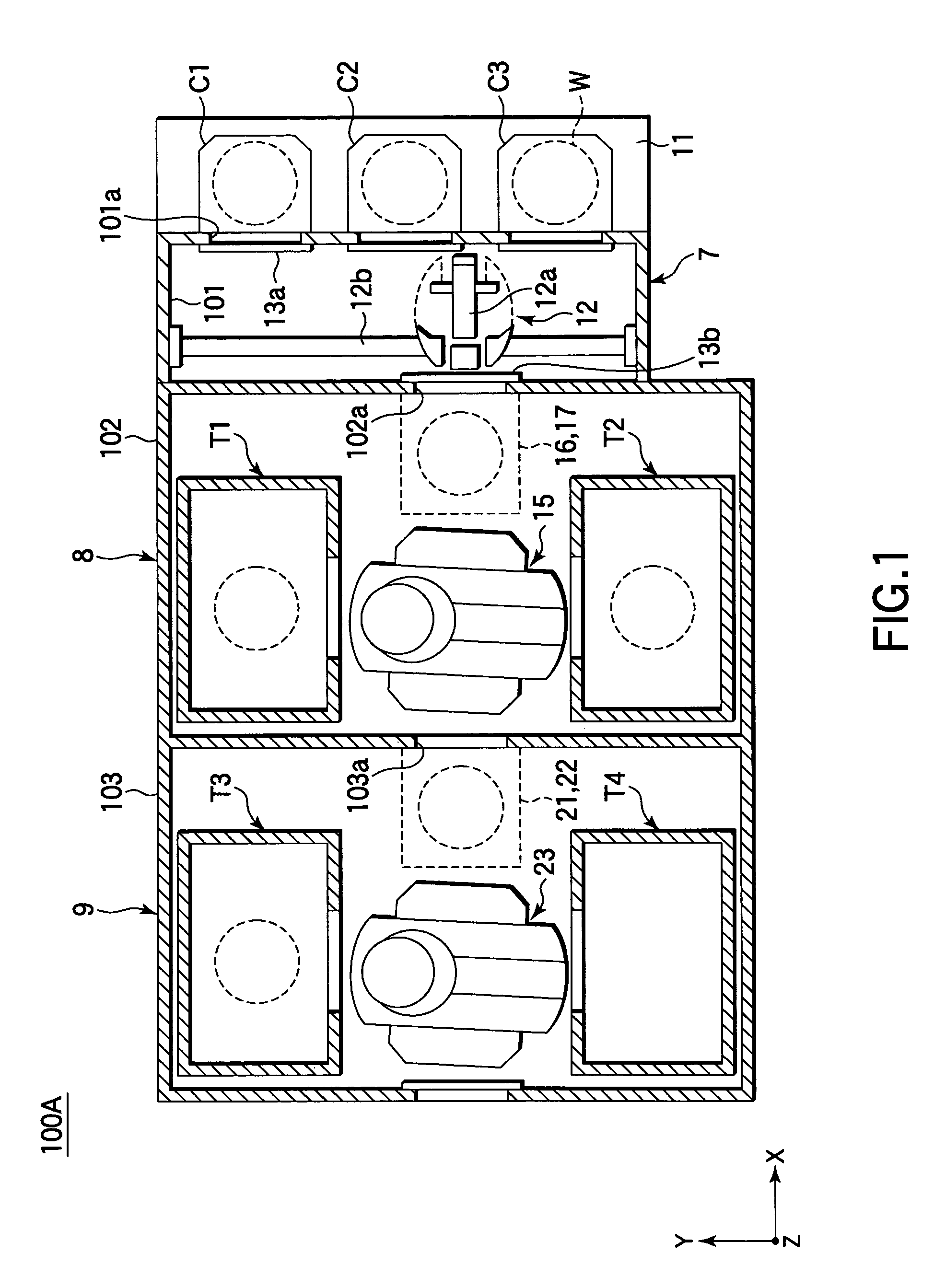
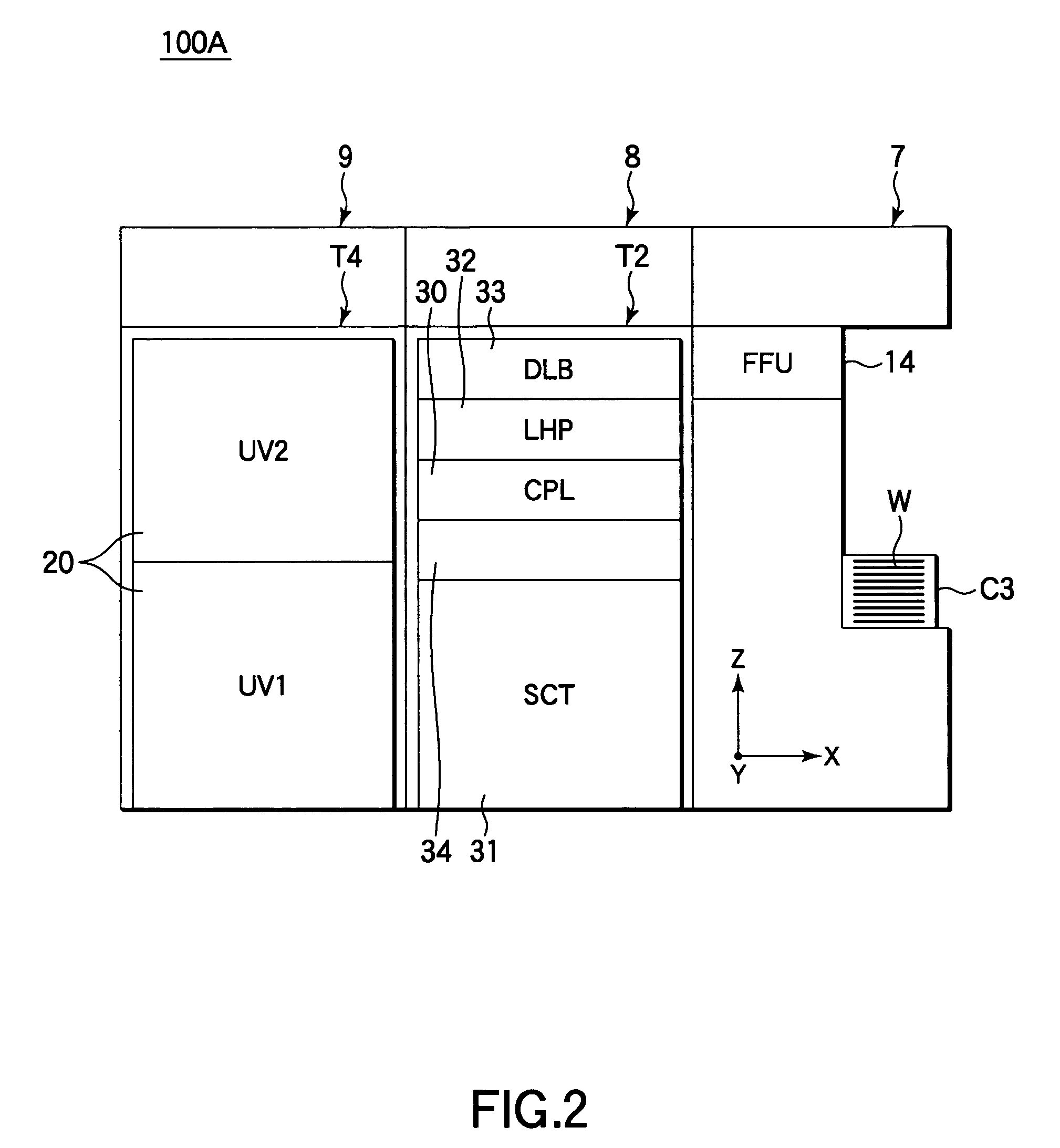
[0027]Embodiments of the present invention will now be described with reference to the accompanying drawings. FIG. 1 is a plan view schematically showing the structure of an SOD system including a UV curing block which is a substrate processing apparatus according to an embodiment of the present invention. FIG. 2 is a side view of the SOD system shown in FIG. 1.

[0028]The SOD system 100A includes process blocks 8 and 9 for performing predetermined processes on wafers W. The SOD system 100A further includes a carrier block 7 for transferring carriers C1 to C3, each storing a predetermined number of wafers W, therethrough relative to the outside, and for transferring wafers W between the carriers C1 to C3 and process block 8.

[0029]The carrier block 7 includes a carrier table 11, on which, for example, three carriers C1 to C3 can be placed in a row in a Y-direction. The carrier block 7 is provided with a transfer device 12 disposed in the casing 101 to transfer wafers W between the carr...


PUM


Abstract

A substrate processing apparatus is used for radiating UV rays onto a target film formed on a target surface of a substrate to perform a curing process of the target film. The apparatus includes a hot plate configured to heat the substrate to a predetermined temperature, a plurality of support pins disposed on the hot plate to support the substrate, and a UV radiating device configured to radiate UV rays onto the target surface of the substrate supported on the support pins. The support pins are preset to provide a predetermined thermal conductivity to conduct heat of the substrate to the hot plate. The hot plate is preset to have a predetermined thermal capacity sufficient to absorb heat conducted through the support pins.

Description

BACKGROUND OF THE INVENTION[0001]1. Field of the Invention[0002]The present invention relates to a substrate processing apparatus and method for performing a curing process on a target film formed on a substrate, such as a semiconductor wafer, to cure the target film.[0003]2. Description of the Related Art[0004]As a method for forming an inter-level insulating film on, e.g., a semiconductor wafer (which may be referred to as “wafer”), in the process of manufacturing semiconductor devices, there is an SOD (Spin on Dielectric) method that comprises steps of forming a coating film on a wafer by spin coating and performing a chemical process or heating process on the film, thereby forming an inter-level insulating film.[0005]According to this method, at first, a coating liquid formed of a solvent with a material dispersed therein for forming an insulating film is applied on the surface of a wafer, and then the solvent of the coating liquid is dried up. Then, the coating film (target fil...

Claims


Application Information

Patent Timeline
Patent Type & Authority Patents(United States)
IPC IPC(8): H01L21/00
CPCH01L21/3105H01L21/67115H01L21/68742H01L21/67225Y10T117/1016
Inventor SATOH, NAOYUKITAMURA, TAKESHIIDE, HIROYUKIHAMA, MANABU
Owner TOKYO ELECTRON LTD
Why Eureka
Try Eureka