
Precision pulse generator

a pulse generator and precision technology, applied in the field of pulse generating circuits, can solve the problems of consuming more power by the larger device than its smaller counterpart, generating/distributing signals more efficiently, and reducing the efficiency of the generating delay

Active Publication Date: 2011-01-18
ORACLE INT CORP
View PDF6 Cites 2 Cited by
  • Summary
  • Abstract
  • Description
  • Claims
  • Application Information

AI Technical Summary

Benefits of technology

"The patent describes a circuit and method for generating pulses based on a clock signal. The circuit includes a precharge circuit to prepare a storage node for a logic signal, a logic circuit to produce the pulse based on the clock signal, and a discharge circuit to control the timing of the pulse. The technical effect of this invention is to provide a reliable and efficient way to generate pulses with precise timing and duration."

Problems solved by technology

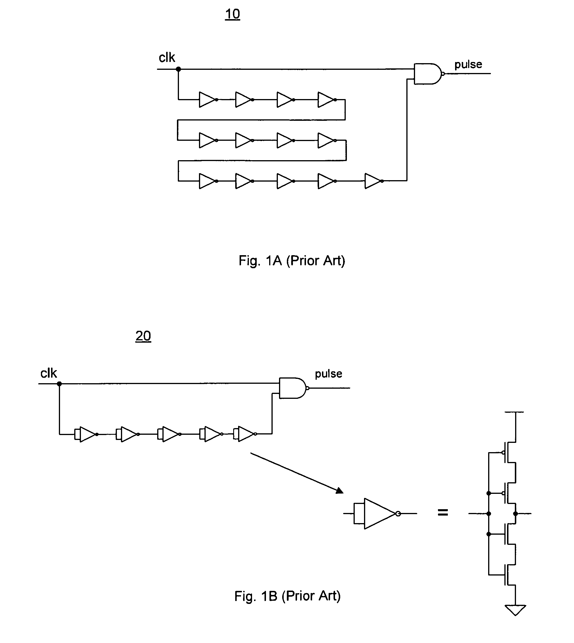
Such an inverter configuration may provide a higher input capacitance and lower drive may thus generate delay more efficiently than the typical inverter configuration having only one PMOS device and one NMOS device.
However, smaller devices are more subject to process variation during manufacturing.
However, larger devices typically consume more power than their smaller counterparts.

Method used


Image

  • Precision pulse generator
  • Precision pulse generator
  • Precision pulse generator

Examples


Embodiment Construction

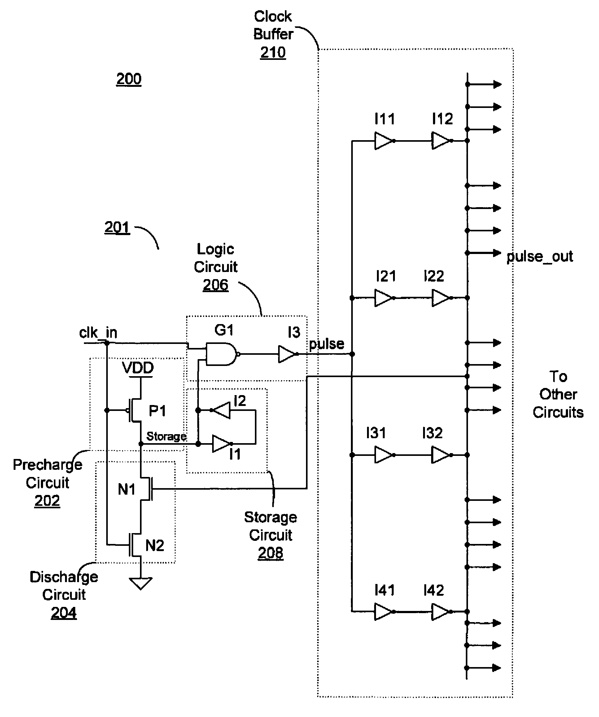
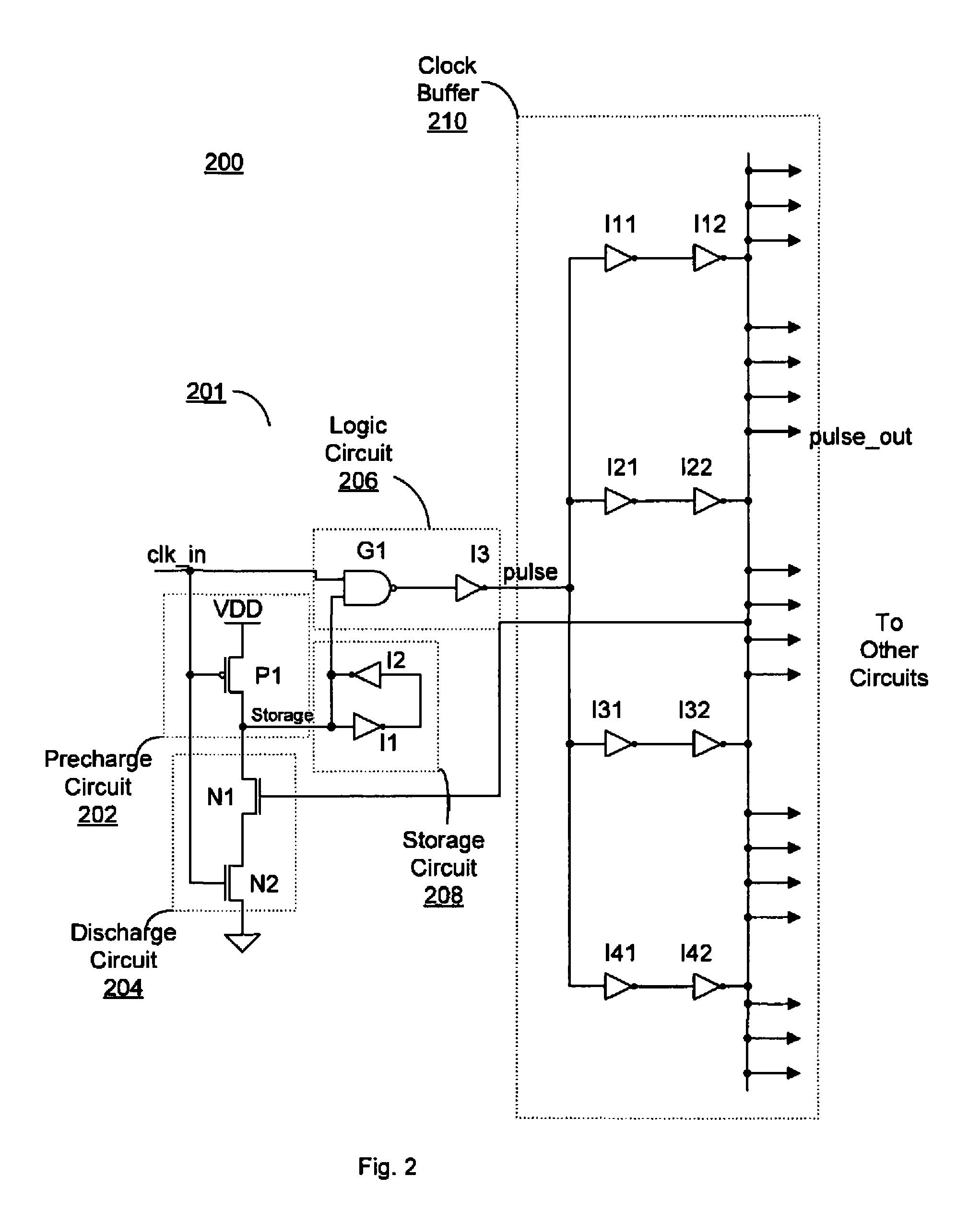
[0018]Turning now to FIG. 2, a schematic diagram of one embodiment of a pulse generator circuit coupled to receive feedback from a node of an associated clock buffer circuit is shown. In the embodiment shown, electronic circuit 200 includes pulse generator circuit 201 and clock buffer 210. Pulse generator circuit 201 in this embodiment includes a precharge circuit 202, a discharge circuit 204, a logic circuit 206, and a storage circuit 208.

[0019]Precharge circuit 202 in the embodiment shown includes transistor P1. When the input clock signal, clk_in, is low, transistor P1 is activated. When transistor P1 is turned on, a pull-up path exists between the storage node (‘storage’) and VDD. Thus, the storage node is precharged to a logic high value during the low portion of the clock cycle in this embodiment. The precharge is discontinued when the input clock signal transitions to a logic high by deactivating transistor P1. However, the logic high value may be captured and initially held ...


PUM


Abstract

A pulse generator circuit. The pulse generator circuit includes a precharge circuit coupled to receive a clock signal alternating between a first logic level and a second logic level, a storage circuit having a storage node, wherein the precharge circuit is configured to precharge the storage node when the clock signal is at the first logic level, a logic circuit having an output, a first input node coupled to receive the clock signal, and a second input node coupled to the storage node and configured to produce a pulse at the second logic level responsive to the clock signal transitioning to the second logic level, and a discharge circuit configured to discharge the storage node at a predetermined delay time subsequent to the clock signal transitioning to the second logic level, wherein the output of the logic circuit transitions to the first logic level responsive to discharging the storage node.

Description

BACKGROUND OF THE INVENTION[0001]1. Field of the Invention[0002]This invention relates to electronic circuits, and more particularly, to pulse generating circuits.[0003]2. Description of the Related Art[0004]Pulse generating circuits are well known in the art of electronics. Pulse generators may be defined by such factors as pulse repetition rate (i.e. frequency), pulse width, trigger delay, duty cycle, rise and fall times, and voltage levels (i.e. of high and low signals).[0005]FIG. 1A is a schematic diagram of one embodiment of a pulse generator circuit. In the embodiment shown, pulse generator 10 includes a NAND gate and an odd number of inverters coupled in series to form a delay chain. A clock input (‘clk’) is provided directly to one of the inputs of the NAND gate, and is also input into the delay chain. When the input clock signal and the delayed clock signal are both high, the output of the NAND gate will fall low. The low from the NAND gate may be provided to a clock header...

Claims


Application Information

Patent Timeline
Patent Type & Authority Patents(United States)
IPC IPC(8): H03K3/013
CPCH03K3/011H03K3/012H03K3/355H03K2005/00293
Inventor MASLEID, ROBERT PGREENHILL, DAVID
Owner ORACLE INT CORP
Learn More