Method for manufacturing semiconductor device

a semiconductor and integrated circuit technology, applied in the field of semiconductor devices, can solve the problems of low resistance to external stress in the integrated circuit of the semiconductor that is reduced in size and thickness, and achieve the effect of less connection failure and high resistance to external stress

Inactive Publication Date: 2011-02-08
SEMICON ENERGY LAB CO LTD
View PDF54 Cites 21 Cited by
  • Summary
  • Abstract
  • Description
  • Claims
  • Application Information

AI Technical Summary

Benefits of technology

[0007]As described above, when a semiconductor integrated circuit is manufactured by transferring a semiconductor element layer separated from a semiconductor substrate, the size and thickness of the semiconductor integrated circuit can be reduced without increasing the area thereof.
[0008]However, a semiconductor integrated circuit that is reduced in size and thickness has a disadvantage of low resistance to external stress.
[0009]As a material for protecting such a semiconductor integrated circuit, a prepreg is known which uses an organic resin and a sheet-like fiber body such as glass cloth. The prepreg is a strong protective material, which can prevent damage of a semiconductor element layer in a semiconductor integrated circuit that is reduced in thickness.

Problems solved by technology

However, a semiconductor integrated circuit that is reduced in size and thickness has a disadvantage of low resistance to external stress.

Method used


Image

  • Method for manufacturing semiconductor device
  • Method for manufacturing semiconductor device
  • Method for manufacturing semiconductor device

Examples


embodiment 1

[0041]This embodiment will be described with reference to FIGS. 1A to 1F, FIGS. 2A to 2D, FIGS. 3A to 3E, FIGS. 4A to 4D, FIGS. 5A to 5D, FIGS. 6A to 6C, FIGS. 7A to 7C, FIGS. 8A and 8B, FIG. 9, FIG. 10, and FIGS. 11A and 11B.

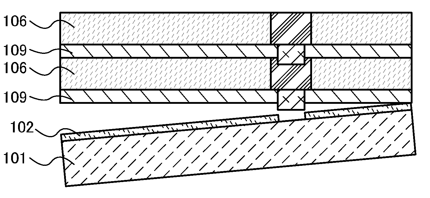
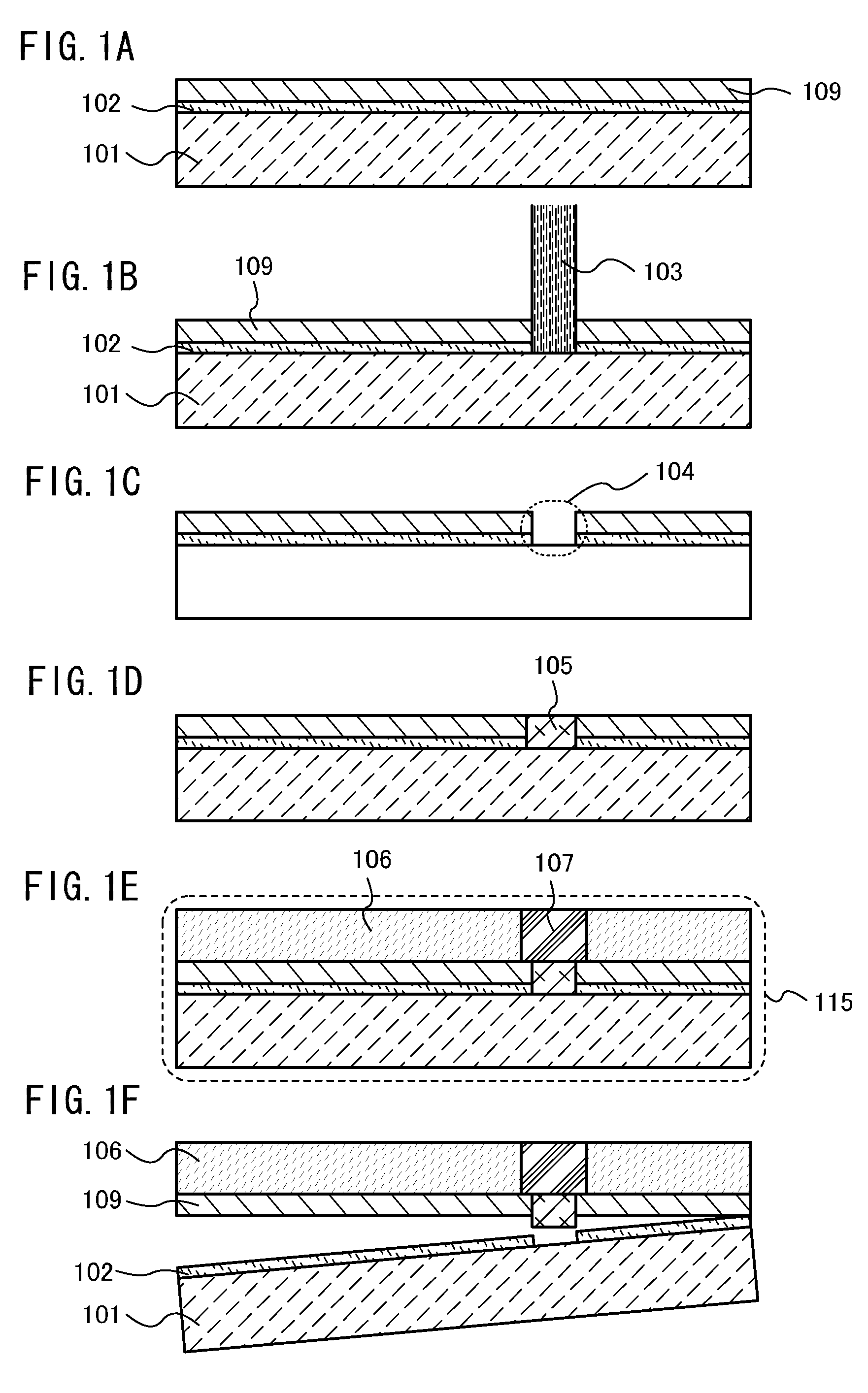
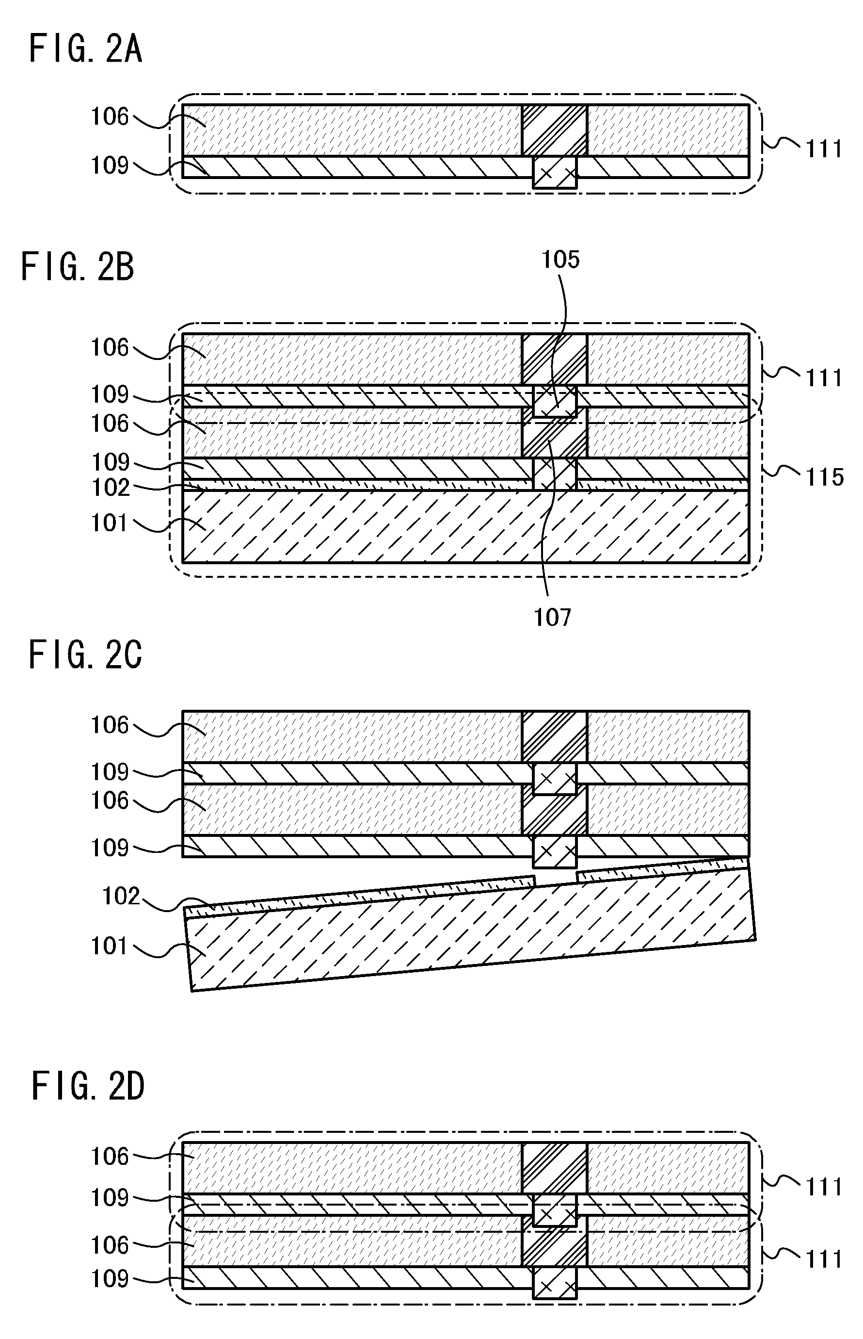
[0042]First, a basic manufacturing process of this embodiment will be described with reference to FIGS. 1A to 1F and FIGS. 2A to 2D. After a separation layer 102 is formed over a substrate 101, a semiconductor element layer 109 is formed over the separation layer 102 (see FIG. 1A).

[0043]Then, a laser beam 103 is emitted from above the semiconductor element layer 109 (see FIG. 1B), whereby a part of the semiconductor element layer 109 and a part of the separation layer 102 are removed to form an opening 104 (see FIG. 1C).

[0044]After that, a wiring 105 is formed in the opening 104 to be electrically connected to the semiconductor element layer 109 (see FIG. 1D).

[0045]Then, a protective material 106 is formed over the semiconductor element layer 109, and an electr...


PUM


Abstract

A method for manufacturing a thin but robust stack of electrically connected thin film semiconductor elements includes the steps of forming a first element to be stacked: forming a separation layer and a semiconductor element layer over a substrate, forming a wiring connected to the semiconductor element layer, forming a protective material over the semiconductor layer and the wiring, forming a conductive region electrically connected to the wiring in the protective layer, and separating the semiconductor element layer from the substrate along the separation layer. A second element is formed according to the aforementioned process, and the first element is stacked thereon, before separating the second element from its substrate. The first element is bonded to the protective layer of the second element so that the semiconductor element layers of the first and the second element are electrically connected to each other through the protective layer, without damaging the protective layer.

Description

BACKGROUND OF THE INVENTION[0001]1. Field of the Invention[0002]The invention disclosed in this specification relates to a semiconductor device and a method for manufacturing the same.[0003]2. Description of the Related Art[0004]Advances in semiconductor manufacturing technologies have allowed large-scale integrated circuits to be more highly integrated, and demand for LSI systems (LSI: Large Scale Integration), in which a plurality of functions is integrated on a silicon chip, has increased. In recent years, three-dimensional LSI systems consisting in a stack of a plurality of LSI chips have been developed to be ready for sophisticated and complicated systems. The 3D LSI systems are also referred to as multi-chip packages because a package includes a plurality of LSIs.[0005]Another technology has also been developed: a semiconductor element layer separated from a semiconductor substrate is transferred on another substrate by a transfer method; and a semiconductor element layer sepa...

Claims


Application Information

Patent Timeline
Patent Type & Authority Patents(United States)
IPC IPC(8): H01L21/60
CPCH01L21/6835H01L21/76802H01L21/76898H01L24/03H01L24/05H01L24/11H01L24/12H01L24/16H01L25/0657H01L24/83H01L2221/68372H01L2224/1147H01L2224/13009H01L2224/13099H01L2224/29499H01L2224/83851H01L2225/06513H01L2225/06541H01L2225/06589H01L2924/01002H01L2924/01004H01L2924/01005H01L2924/01007H01L2924/0101H01L2924/01013H01L2924/01014H01L2924/01018H01L2924/01022H01L2924/01027H01L2924/01028H01L2924/01029H01L2924/0103H01L2924/0104H01L2924/01042H01L2924/01046H01L2924/01047H01L2924/01058H01L2924/0106H01L2924/01073H01L2924/01074H01L2924/01077H01L2924/01078H01L2924/01079H01L2924/05042H01L2924/10329H01L2924/14H01L2924/01006H01L2924/01024H01L2924/01033H01L2924/01041H01L2924/01044H01L2924/01045H01L2924/01067H01L2924/01068H01L2924/01072H01L2924/01076H01L2224/16147H01L2224/1601H01L2224/16237H01L2224/29076H01L2224/81191H01L2224/0401H01L2224/0554H01L2924/10253H01L2924/00H01L2924/15787H01L2924/15788H01L2924/12044
Inventor CHIDA, AKIHIRO
Owner SEMICON ENERGY LAB CO LTD
Why Eureka
Try Eureka