Optically initiated silicon carbide high voltage switch

a silicon carbide, high-voltage switch technology, applied in the direction of electrographic process, instrumentation, corona discharge, etc., can solve the problems of short lifetime and variable failure mechanisms

Inactive Publication Date: 2011-02-22
LAWRENCE LIVERMORE NAT SECURITY LLC
View PDF2 Cites 11 Cited by
  • Summary
  • Abstract
  • Description
  • Claims
  • Application Information

AI Technical Summary

Problems solved by technology

The difficulty with these materials is that various failure mechanisms occur even at modest parameters.
Thus, the principal issue with photoconductive switching has been short lifetime resulting from overstressing current and voltage conditions.

Method used


Image

  • Optically initiated silicon carbide high voltage switch
  • Optically initiated silicon carbide high voltage switch
  • Optically initiated silicon carbide high voltage switch

Examples


Embodiment Construction

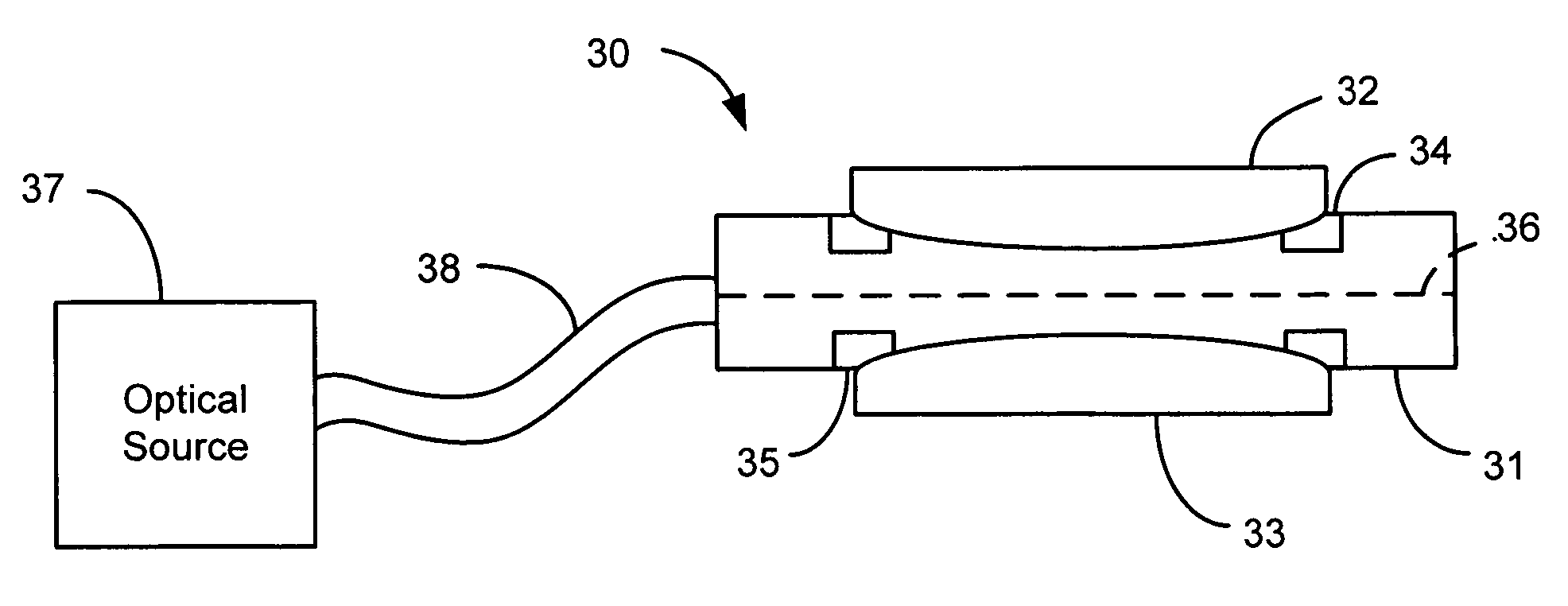
[0029]The photoconductive switch of the present invention improves upon the basic photoconductive switch construction and operation shown in FIG. 7, with enhancements enabling the switch to handle high voltages and high currents with minimum inductance, rapid closure, precise temporal control and the possibility of long life. As such, the photoconductive switch of the present invention shares much the same construction as a basic photoconductive switch shown in FIG. 7 generally having a photoconductive material 21 between two electrodes 22 and 23. Without optical energy injection, i.e. in the dark, the photo-conductive material is an insulator with a large resistance value (much larger than the circuit impedance) and thus the switch essentially blocks current flow. When optical energy is injected and absorbed in the photoconductive material, the switch resistance drops to a small value (much less than the circuit impedance) and the switch conducts current. Thus the basic photoconduc...


PUM

PropertyMeasurementUnit
dielectric strengthaaaaaaaaaa
photoconductiveaaaaaaaaaa

Abstract

An improved photoconductive switch having a SiC or other wide band gap substrate material, such as GaAs and field-grading liners composed of preferably SiN formed on the substrate adjacent the electrode perimeters or adjacent the substrate perimeters for grading the electric fields.

Description

I. REFERENCE TO PRIOR APPLICATIONS[0001]This application claims the benefit of U.S. Provisional Application No. 60 / 730,161, filed Oct. 24, 2005, and U.S. Provisional Application No. 60 / 798,016, filed May 4, 2006, all of which are incorporated by reference herein.[0002]The United States Government has rights in this invention pursuant to Contract No. W-7405-ENG-48 between the United States Department of Energy and the University of California for the operation of Lawrence Livermore National Laboratory.II. FIELD OF THE INVENTION[0003]The present invention relates to photoconductive switches and more particularly to an optically initiated silicon carbide (SiC) high voltage switch.III. BACKGROUND OF THE INVENTION[0004]Particle accelerators, such as for example dielectric wall accelerators (DWA), are critically dependent upon high voltage, high current, fast closing switches that can be activated with nanosecond precision. Photoconductive switches offer the most potential in terms of han...

Claims


Application Information

Patent Timeline
Patent Type & Authority Patents(United States)
IPC IPC(8): H01L23/48H01L23/52H01L29/40
CPCH01L31/09H05H7/00G03G15/02
Inventor CAPORASO, GEORGE J.SAMPAYAN, STEPHEN E.SULLIVAN, JAMES S.SANDERS, DAVID M.
Owner LAWRENCE LIVERMORE NAT SECURITY LLC
Why Eureka
Try Eureka