Trench IGBT with trench gates underneath contact areas of protection diodes

a technology of protection diodes and trench gates, which is applied in the direction of diodes, semiconductor devices, electrical apparatus, etc., can solve the problems of low yield and reliability, and the shortage of etching etching etching problems, so as to reduce contact resistance, no additional cost, and widen the trench width

Inactive Publication Date: 2011-03-01
FORCE MOS TECH CO LTD
View PDF4 Cites 21 Cited by
  • Summary
  • Abstract
  • Description
  • Claims
  • Application Information

AI Technical Summary

Benefits of technology

[0009]One advantage of the present invention is that, additional trench gates with a wider trench width than the trench contacts are applied in a lightly doped epitaxial layer right below trench contacts in ESD protection diodes as buffer trenched gates. By employing this configuration, no shortage issue will happen even if over etching takes place during the manufacturing process because the trench contacts touch the buffer trenched gates instead of the lightly doped epitaxial layer.
[0010]Another advantage of the present invention is that, no additional cost is required to implement the trench gates underneath contact areas of protection diodes since the trench gates can be formed at the same step as other trench gates formed.
[0011]Another advantage of the present invention is that, the inventive structure is suitable for both PT IGBT and NPT IGBT with G-C Clamp Diodes or with G-E Clamp Diodes or with G-C and G-E Clamp Diodes.
[0012]Briefly, in a preferred embodiment, as shown in FIG. 3B, the present invention discloses a trench PT IGBT cell with G-E Clamp Diodes for G-E ESD protection. The transistor cell comprises: a first epitaxial layer moderately doped with a first semiconductor doping type (e.g., N dopant) grown onto a substrate heavily doped with a second semiconductor doping type (e.g., P dopant) coated with a back metal on its rear side; a second epitaxial layer lightly doped with the same doping type as the first epitaxial layer and grown whereon; a plurality of trenches and at least a wider trench etched within the second epitaxial layer and filled with doped poly over a gate oxide layer to form trench gates and at least a wider trench gate for gate connection; base regions formed within the top portion of the second epitaxial layer and moderately doped with the opposite doping type to epitaxial layer; emitter regions heavily doped with the same doping type as the epitaxial layer near the front surface of base region between two adjacent trench gates; a doped polysilicon layer overlying a portion of the insulating layer as ESD protection diodes comprising multiple back to back Zener diodes which composed of doping areas of a first semiconductor doping type next to doping areas of a second semiconductor doping type; trench contacts penetrating through a thick dielectric interlayer and emitter, and extending into base regions, two cathodes of ESD protection diodes, and at least a wider trench gate to electrically connect the emitter regions, the base regions and one cathode of ESD protection diodes to the emitter metal, and to electrically connect the trench gate and another cathode of ESD protection diodes to the gate metal, respectively; an area heavily doped with the same doping type as base region around each bottom of trench emitter contact and trench base contact to reduce contact resistance between base region and metal plug filled in trench contacts. Specially, additional trench gates are formed right underneath each trench contact of the ESD protection diodes as a buffer layer to avoid G-E shortage issue.
[0013]Briefly, in another preferred embodiment, as shown in FIG. 4B, the present invention discloses a trench PT IGBT cell with G-C Clamp Diodes for G-C protection. Different from configuration in FIG. 3B, here one cathode of the ESD protection diodes is connected to gate metal while another is connected to collector metal. However, despite all that, there are still inventive trench gates right underneath each trench contact of G-C protection diodes to ward off the happening of shortage issue between G-C, or G-E, or G-C-E resulted from trench contacts of ESD protection over etching to base regions.
[0014]Briefly, in another preferred embodiment, as shown in FIG. 5B, the present invention discloses a trench PT IGBT cell with both G-E and G-C Clamp Diodes for G-E and G-C ESD protection, respectively. The pluralities of Zener Diodes contain at least three cathodes to be connected to gate metal, emitter metal and collector metal, respectively. Underneath each trench contact of protection diodes, a trench gate is formed to ward off the shortage of gate and collector to emitter resulted from trench contacts of ESD protection over etching to base regions.

Problems solved by technology

Though trench contacts employed in this prior art have better connection stability and higher device density than planar contact used in other conventional art, it will still encounter another hazardous shortage issue, which happens between gate and emitter when trench contacts 127 and 128 are over etched through ESD protection diodes and thin oxide layer 136 and into P base region 104 during fabrication process, causing accordingly low yield and reliability issues, as shown in FIG. 2.
Unfortunately, this shortage problem induced by over etching may also be found in cases when G-C clamp diodes are applied as well as in conventional trench NPT IGBT with protection diodes.

Method used


Image

  • Trench IGBT with trench gates underneath contact areas of protection diodes
  • Trench IGBT with trench gates underneath contact areas of protection diodes
  • Trench IGBT with trench gates underneath contact areas of protection diodes

Examples


Embodiment Construction

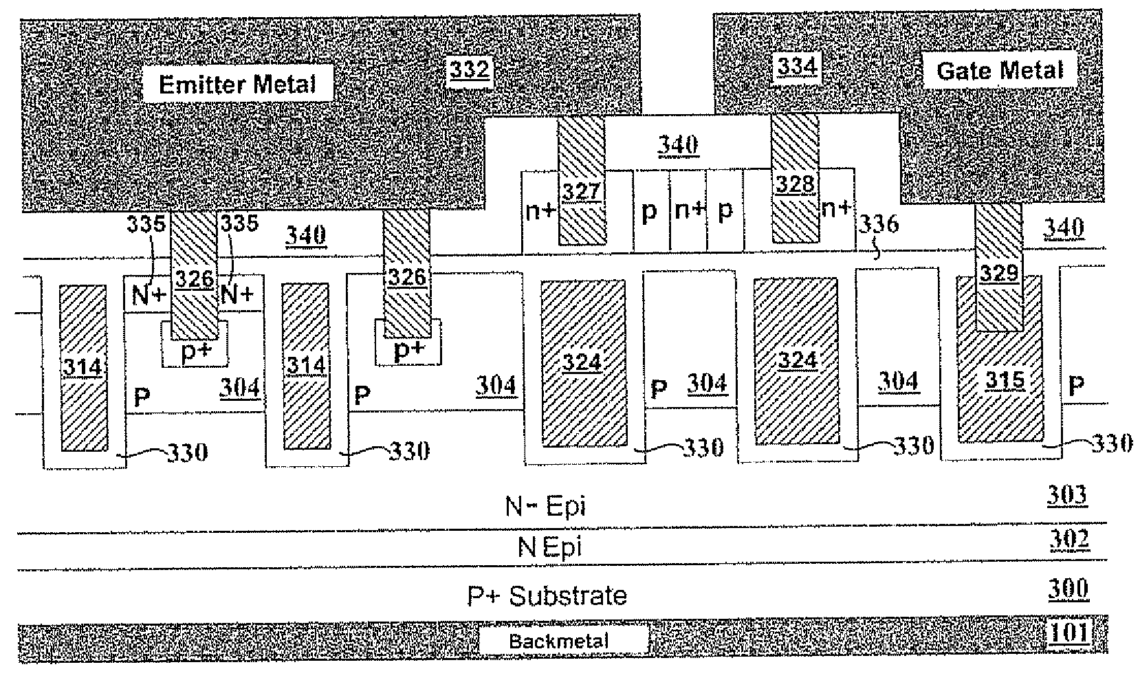
[0029]Please refer to FIG. 3A to FIG. 3B for a circuit diagram and a side cross sectional view respectively of a first preferred embodiment of this invention where a trench PT IGBT device cell with a gate-emitter polysilicon Zener clamp diodes for ESD protection is disclosed. The transistor cell is formed on a P+ substrate 300 coated with a back metal 301 on its rear side. Onto said substrate 300, a moderately N doped epitaxial layer 302 and a lightly N doped epitaxial layer 303 is successively grown. The trench PT IGBT device further includes trenched gates 314 at least a wider trenched gate 315 and at least two wider trenched gates 324 disposed in epitaxial layer 303 with gate insulation layer 330 formed over the walls of the trenches. Base region 304 which is doped with P dopant, extends among the trenched gates 314, 315 and 324 with N+ emitter regions 335 near the top surface of the base region between two adjacent trenched gates. In order to form G-E protection Zenwe diodes, a ...


PUM


Abstract

A trench PT IGBT (or NPT IGBT) having clamp diodes for ESD protection and prevention of shortage among gate, emitter and collector. The clamp diodes comprise multiple back-to-back Zener Diode composed of doped regions in a polysilicon layer doped with dopant ions of a first conductivity type next to a second conductivity type disposed on an insulation layer above said semiconductor power device. Trench gates are formed underneath the contact areas of the clamp diodes as the buffer layer for prevention of shortage.

Description

CROSS REFERENCE TO RELATED APPLICATION[0001]This application is a continuation in part of U.S. patent application Ser. No. 12 / 036,248 filed on Feb. 23, 2008BACKGROUND OF THE INVENTION[0002]1. Field of the Invention[0003]This invention relates generally to the cell structure, device configuration and fabrication process of trench Punch-Through insulated gate bipolar transistor (PT IGBT) and trench Non Punch-Through insulated gate bipolar transistor (NPT IGBT). More particularly, this invention relates to an improved device configuration and process to manufacture PT IGBT and NPT IGBT with ESD (electrostatic discharge) protection having the characteristics of preventing emitter, gate and collector shortage issue from happening.[0004]2. Description of the Related Art[0005]In order to enhance the ESD protection for trench PT IGBT and NPT IGBT, many different configurations are disclosed in prior arts with G-E Clamp Diodes or G-C Clamp Diodes or with G-E and G-C Clamp Diodes for G-E and ...

Claims


Application Information

Patent Timeline
Patent Type & Authority Patents(United States)
IPC IPC(8): H01L29/739
CPCH01L27/0255H01L29/66348H01L29/7397
Inventor HSIEH, FU-YUAN
Owner FORCE MOS TECH CO LTD
Why Eureka
Try Eureka