Solid state imaging device and manufacturing method thereof

a manufacturing method and imaging device technology, applied in the direction of color television, television system, radio control device, etc., can solve the problems of warpage of several millimeters, substrate breakage, and adhesive cure requires heat to be cured, so as to prevent warpage or breakage, reduce process and cost of manufacturing the solid state imaging device, and improve the effect of thermal expansion

Inactive Publication Date: 2011-03-08
FUJIFILM CORP
View PDF20 Cites 15 Cited by
  • Summary
  • Abstract
  • Description
  • Claims
  • Application Information

AI Technical Summary

Benefits of technology

[0013]It is preferable that the coefficient of thermal expansion of the optical plate is 2 ppm / ° C. to 5 ppm / ° C., which is approximately equal to that of a typical image sensor chip formed of silicon. In addition, to regulate the thermal expansion of the cover glass by the optical plate and prevent a breakage of joint between each components, it is preferable that the cover glass is a low-α-ray glass whose coefficient of thermal expansion is approximately the same as or larger than the optical plate.
[0018]According to the solid state imaging device of the present invention, since the optical plate whose coefficient of thermal expansion is approximately equal to the image sensor chip is attached on the cover glass, the thermal expansion of the cover glass is regulated to prevent warpage or breakage in the components of the solid state imaging device due to heat in the image capturing operation. In addition, since the low-α-ray glass for the cover glass has the coefficient of thermal expansion approximately same as or larger than the optical plate, the thermal expansion thereof can be regulated more effectively.
[0019]Since the optical plate is the infrared cut filter, the optical low pass filter, the anti-reflection filter or the like, processes and cost for manufacturing the solid state imaging device can be reduced compared to the conventional method. In addition, since the image sensor and the spacer are joined by the heat cure adhesive having the glass transition point of at least 120° C., current leak does not occur and the light receiving section can be properly sealed even in high temperature and high humidity conditions.
[0020]According to the manufacturing method of the solid state imaging device of the present invention, since the support substrate having the coefficient of thermal expansion approximately same as the wafer is attached to the transparent substrate and then the transparent substrate is partially cut off on the support substrate to form the cover glasses, the support substrate is rarely affected by the thermal expansion of the cover glass even when the heat cure adhesive is used. Therefore, the cause of warpage or the breakage due to the difference of the coefficient of thermal expansion between the substrates is prevented.
[0021]In addition, since the attachment of the single support substrate produces the plurality of the solid state imaging device each of which includes the optical plate such as the infrared cut filter, the productivity can be improved.

Problems solved by technology

Since the heat cure adhesive has low reactivity, current leak or other problems do not occur when being used on wiring patterns of the wafer.
However, there is a problem that the heat cure adhesive requires the application of heat to be cured.
Accordingly, when the heat cure adhesive is used for joining of the transparent substrate and the wafer, there is a possibility that a warpage of several millimeters is caused in the joined substrates after the substrates are returned to the room temperature from the high temperature, because of a difference of the coefficient of thermal expansion between the two substrates.
The warpage possibly breaks the substrates, or adversely affects post-processes even when the substrates are not broken.
However, the UV cure adhesive cannot be used for joining of the spacer and the wafer because the spacer is formed of a material such as silicon, which does not transmit UV light.
However, the room-temperature-cure adhesive has high reactivity, which possibly causes current leak or other problems on wiring patterns of the wafer.
Further, since the room-temperature-cure adhesive has low glass transition point (Tg), sealing property and moisture shielding property at high temperature are insufficient.
In addition, the room-temperature-cure adhesive requires long time (for example 16 hours) for being cured, and the productivity becomes worse.
Since the coefficient of thermal expansion is different between the image sensor chip and the cover glass, the junctions between the image sensor chip and the spacer and between the spacer and the cover glass possibly come unstuck because of difference of thermal expansion when being heated.

Method used


Image

  • Solid state imaging device and manufacturing method thereof
  • Solid state imaging device and manufacturing method thereof
  • Solid state imaging device and manufacturing method thereof

Examples


Embodiment Construction

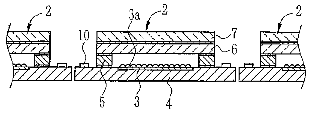
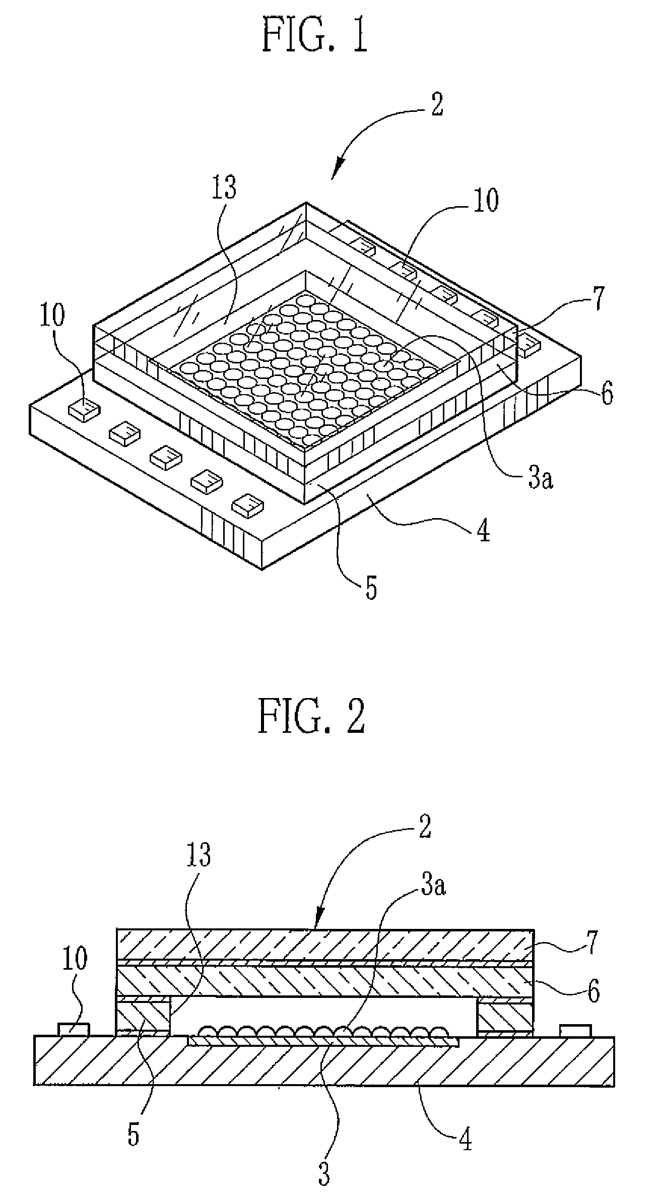
[0033]A construction of the solid state imaging device of the present invention will be described below. As shown in FIG. 1 and FIG. 2, the solid state imaging device 2 comprises an image sensor chip 4 having an upper surface on which a light receiving section 3 is provided, a frame-like spacer 5 attached on the upper surface of the image sensor chip 4 to surround the light receiving section 3, a transparent cover glass 6 attached on the spacer 5 to seal the light receiving section 3, and an infrared cut filter 7 (as an optical plate) attached on the cover glass 6 to cut infrared light.

[0034]The image sensor chip 4 is made by dividing a silicon single crystal wafer into rectangular pieces. On the upper surface of the image sensor chip 4, at the center there is the light receiving section 3 which performs photoelectric conversion, and near two opposite side ends there are plural pads 10 to be connected to a mounting board or the like through wiring. A thickness of the image sensor ch...


PUM


Abstract

To a transparent substrate (20) on which a plurality of spacers (5) are formed, an infrared cut filter (IRCF) substrate (27) is attached. The IRCF substrate (27) has a coefficient of thermal expansion smaller than the transparent substrate (20) and approximately equal to a wafer (31). Next, the transparent substrate (20) is diced into plural pieces to form a plurality of cover glasses (6). Then heat cure adhesive (32) is coated on each spacer (5) and the spacers (5) are attached on the wafer (31) on which a plurality of light receiving section (3) and pads (10) are previously formed. Finally, the heat cure adhesive (32) is heated to be cured.

Description

TECHNICAL FIELD[0001]The present invention relates to a solid state imaging device and a manufacturing method thereof, and more particularly to a solid state imaging device of a chip size package type and a manufacturing method thereof.BACKGROUND ART[0002]To downsize digital cameras, mobile phones and the like, solid state imaging devices incorporated therein are required to be downsized. The conventional solid state imaging devices are formed such that an image sensor chip with a light receiving section is contained in a package of for example a ceramic to be air-tightly sealed. However, recently a solid state imaging device of CSP (Chip Size Package) type is in widespread use. The CSP type solid state imaging device is formed such that a spacer is firstly introduced to surround an outer periphery of a light receiving section on an image sensor chip, and then a transparent cover glass is attached on the spacer to air-tightly seal the light receiving section. Accordingly, the formed...

Claims


Application Information

Patent Timeline
Patent Type & Authority Patents(United States)
IPC IPC(8): H01L21/78H01L27/14H04N5/335
CPCH01L27/14618H01L31/0203H01L2924/0002H01L2924/16235H01L2924/00H01L27/14H01L27/146H04N25/00
Inventor YAMAMOTO, KIYOFUMI
Owner FUJIFILM CORP
Why Eureka
Try Eureka