Light-emitting display

a technology of light-emitting display and display screen, which is applied in the direction of instruments, discharge tube luminescnet screens, static indicating devices, etc., can solve the problems of strong interference, achieve high accuracy of adjustment, improve display quality, and improve manufacturing process efficiency

Active Publication Date: 2011-03-08
SANYO ELECTRIC CO LTD
View PDF22 Cites 49 Cited by
  • Summary
  • Abstract
  • Description
  • Claims
  • Application Information

AI Technical Summary

Benefits of technology

[0007]The present invention aims to reduce the above-described variation in color and luminance in light emitting displays.
[0010]Thus, convexity / concavity is provided in the insulating layer to form the optical path length adjusting section, so that a plurality of optical path lengths can be obtained from the emitting layer to the surface of the substrate on the observation side of the display in one pixel region. Only one optical path length from the emitting layer to the surface of the substrate on the element side in one pixel region leads to only one kind of interference generating condition in the pixel region caused by the optical path length and a predetermined wavelength of emitted light determined by the emissive material used, thereby possibly generating strong interference. As a result, it is more likely to generate variation in color and luminance due to variation in film thickness or the like. By providing a portion having a different optical path length in a pixel, however, the conditions of generating interference are increased, and as a result of combined conditions, the degree of generating interference can be averaged in one pixel, thereby suppressing variation in color and luminance and also color change related to the viewing angle because of the averaged interference.
[0014]According to a further aspect of the present invention, the difference in height in the convexity / concavity is the same in all pixel regions of the plurality of pixels. Consequently, a process for forming the optical path length adjusting section can be performed simultaneously under the same conditions for all pixels, thereby improving efficiency in manufacturing process.
[0015]According to a further aspect of the present invention, the difference in height in the convexity / concavity may be varied in each pixel region of the plurality of pixels in accordance with an associated color. This enables a highly accurate adjustment in accordance with color, i.e. the wavelength of emitted light, thereby further improving display quality.
[0016]According to the present invention, a plurality of interference generating conditions can be set in one pixel to average interference for each pixel, thereby reducing variation in color due to variation in film thickness and color change due to the viewing angle in a very easy and reliable manner.

Problems solved by technology

Only one optical path length from the emitting layer to the surface of the substrate on the element side in one pixel region leads to only one kind of interference generating condition in the pixel region caused by the optical path length and a predetermined wavelength of emitted light determined by the emissive material used, thereby possibly generating strong interference.

Method used


Image

  • Light-emitting display
  • Light-emitting display
  • Light-emitting display

Examples


Embodiment Construction

[0032]Best modes of the present invention (hereinafter referred to as embodiments) will now be described with reference to the accompanying drawings.

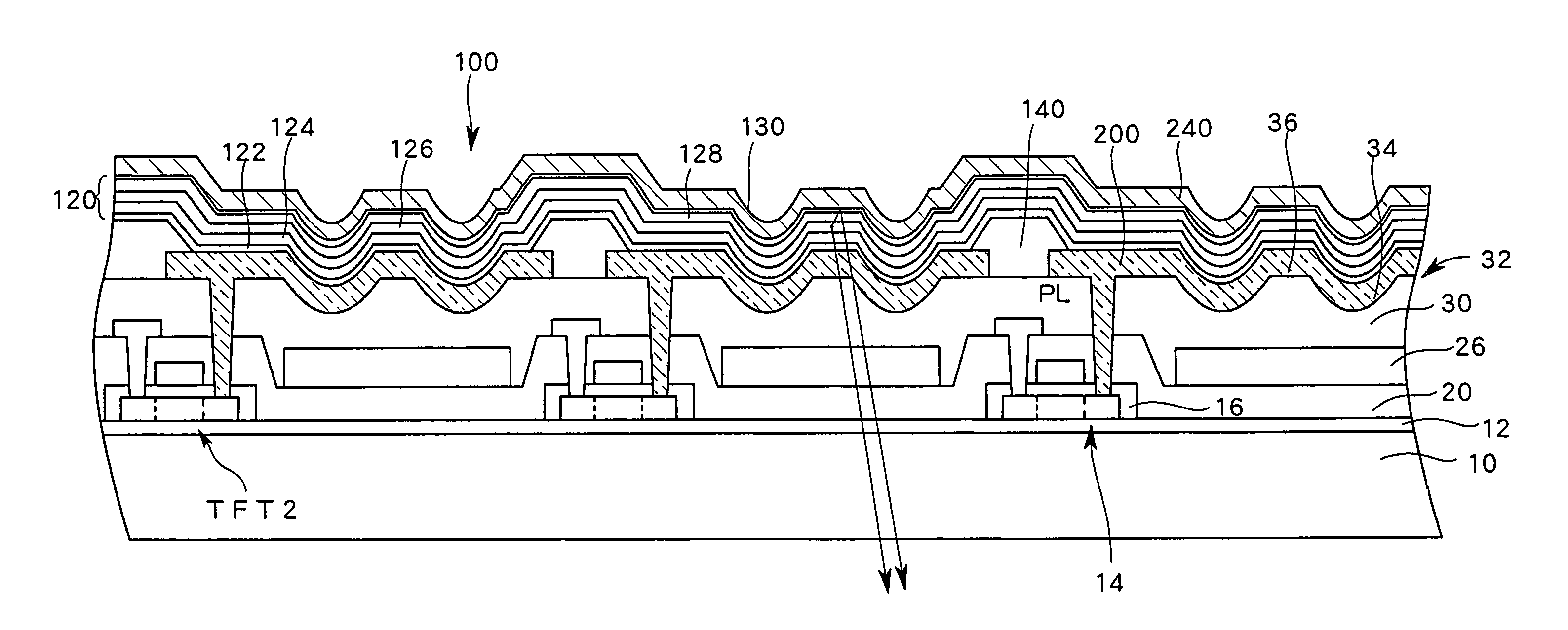
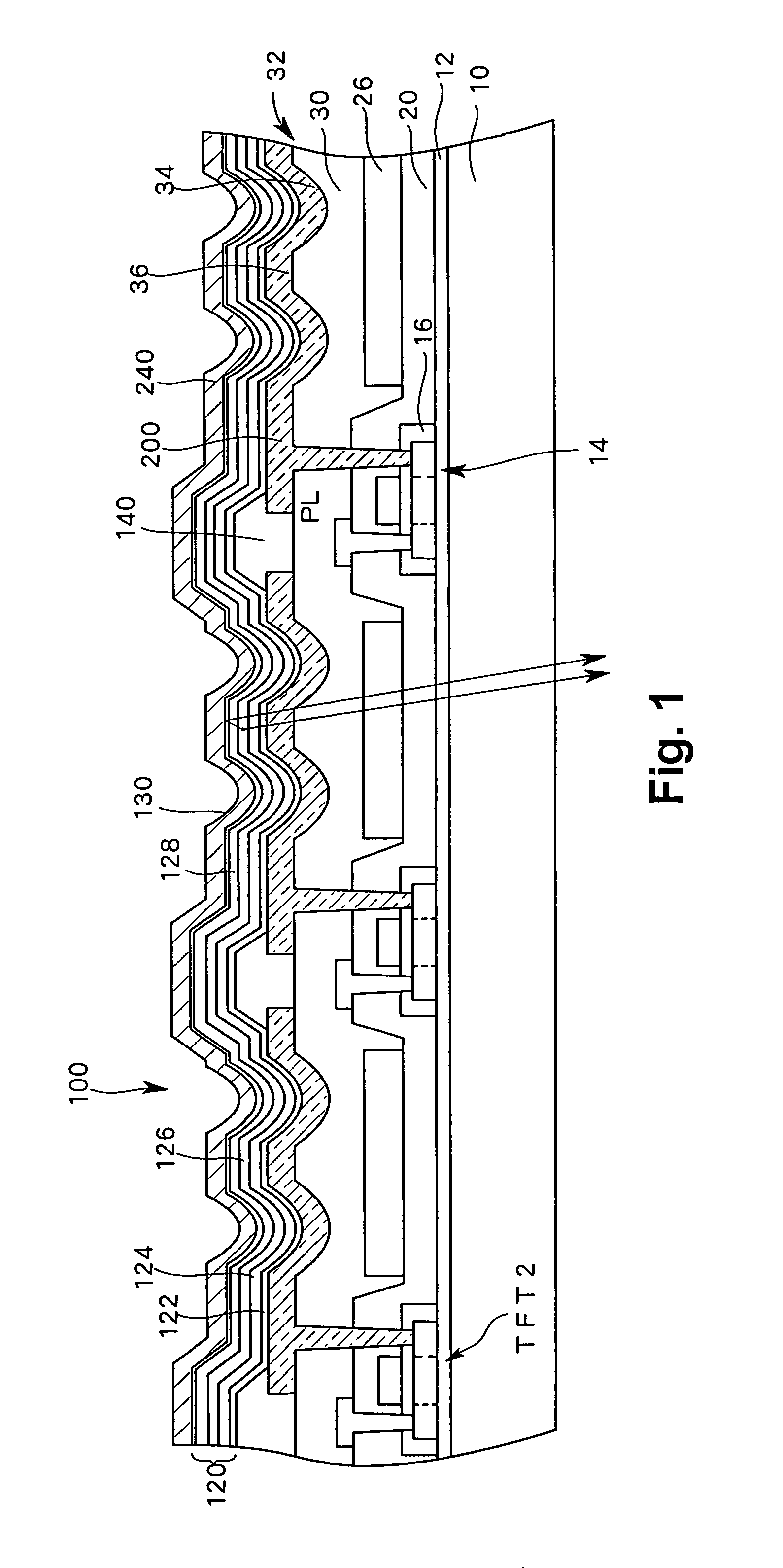
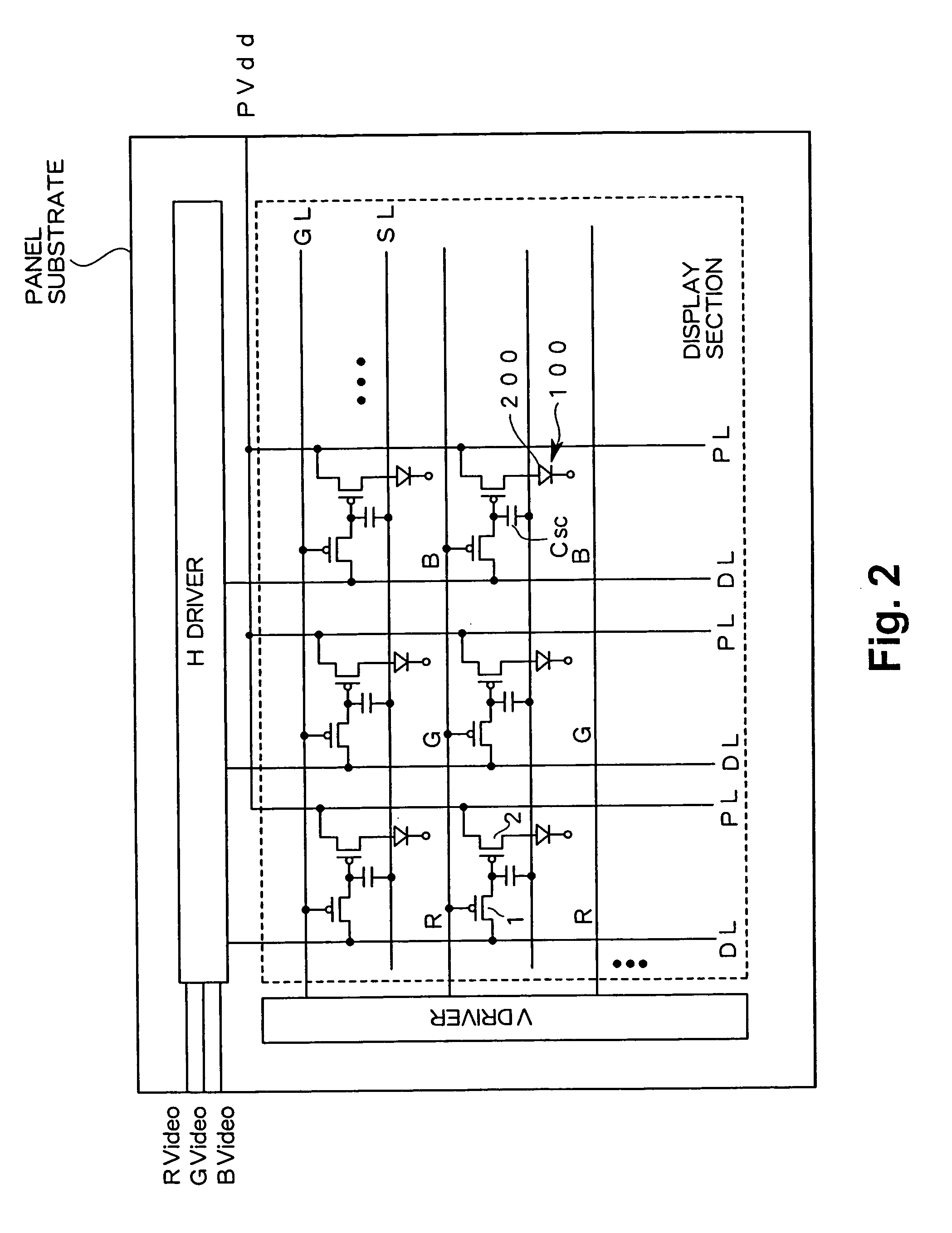
[0033]FIG. 1 schematically shows a cross sectional structure of an important part of a light emitting display device according to an embodiment of the present invention. FIG. 2 shows, as such a light emitting display device, an example of an equivalent circuit of an active matrix type display device having a thin film transistor (TFT) as a switch element controlling an emitting element for each pixel. As a light emitting display device, an organic EL display device using an organic EL element as an emitting element will be described hereinafter as an example.

[0034]In an active matrix type organic EL display device, a plurality of pixels are arranged in a matrix on a transparent substrate 10 formed of glass or the like, and each pixel includes, as illustrated in FIG. 2, an organic EL element 100, a first thin film transistor (hereinafter...


PUM


Abstract

Disclosed is a light-emitting display having a plurality of pixels wherein each pixel comprises a light-emitting device (100) having a light-emitting element layer which is formed between a first electrode and a second electrode and contains at least a light-emitting layer. An insulating layer (30) is formed between the light-emitting device (100) and a surface of a first or second substrate on the viewing side of the display, and the insulating layer (30) is provided with recesses and projections in at least one or more pixel regions, thereby forming an optical path length adjusting portion (32). By forming such an optical path length adjusting portion (32) in a pixel region, there is an increase in the interference conditions for the light emitted from the light-emitting device (100) to the outside, thereby averaging the interference.

Description

CROSS-REFERENCE[0001]This is a U.S. national stage application of International Application No. PCT / JP2005 / 8064, filed on 27 Apr. 2005. Priority under 35 U.S.C. §119(a) and 35 U.S.C. §365(b) is claimed from Japanese Application No. JP2004-135968, filed 30 Apr. 2004, the disclosure of which is also incorporated herein by reference.TECHNICAL FIELD[0002]The present invention relates to a light emitting display, and more particularly to a display including an emitting element for each pixel.BACKGROUND ART[0003]Flat panel displays (FPD) that can be manufactured in reduced size and thickness have been attracting attentions in recent years, and especially a liquid crystal display device, a typical type of the FPDs, has already been employed in a variety of equipments. At present, emissive devices (displays and light sources) using a self-emissive electroluminescence (hereinafter referred to as “EL”) element, particularly organic EL displays capable of emitting light at a high luminance in ...

Claims


Application Information

Patent Timeline
Patent Type & Authority Patents(United States)
IPC IPC(8): G09G3/30H01L27/32H01L51/52H05B33/02H05B33/12H05B33/14
CPCH01L51/5209H01L51/5262H05B33/22H01L27/3213H01L27/322H01L27/3244H01L51/5265H10K59/351H10K59/38H10K59/124H10K50/813H10K50/85H10K50/852H10K2102/351
Inventor NISHIKAWA, RYUJIOMURA, TETSUJI
Owner SANYO ELECTRIC CO LTD
Why Eureka
Try Eureka