Light-Emitting Display

Active Publication Date: 2008-01-31
SANYO ELECTRIC CO LTD
View PDF8 Cites 205 Cited by
  • Summary
  • Abstract
  • Description
  • Claims
  • Application Information

AI Technical Summary

Benefits of technology

[0013] According to a further aspect of the present invention, the difference in height in the convexity/concavity is the same in all pixel regions of the plurality of pixels. Consequently, a process for forming the optical path length adjusting section can be performed simultaneously under the same conditions for all pixels, thereby improving efficiency in manufacturing process.
[0014] According to a further aspect of the present invention, the difference in height in the convexity/concavity may be varied in each pixel r

Problems solved by technology

Only one optical path length from the emitting layer to the surface of the substrate on the element side in one pixel region leads to only one kind of interference generating condition in

Method used


Image

  • Light-Emitting Display
  • Light-Emitting Display
  • Light-Emitting Display

Examples


Embodiment Construction

[0031] Best modes of the present invention (hereinafter referred to as embodiments) will now be described with reference to the accompanying drawings.

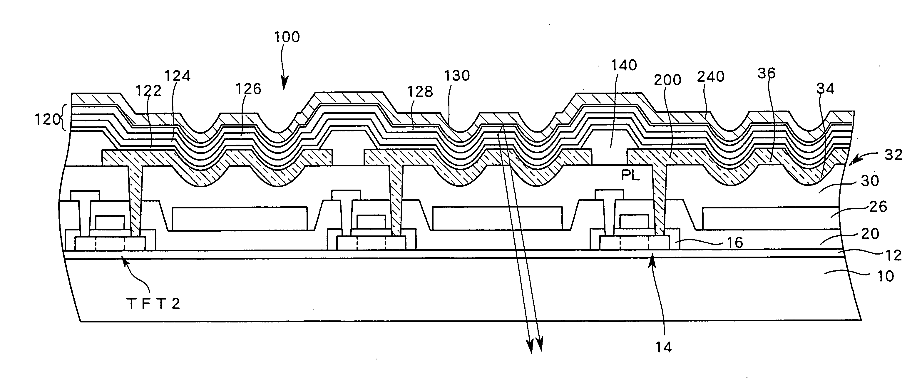
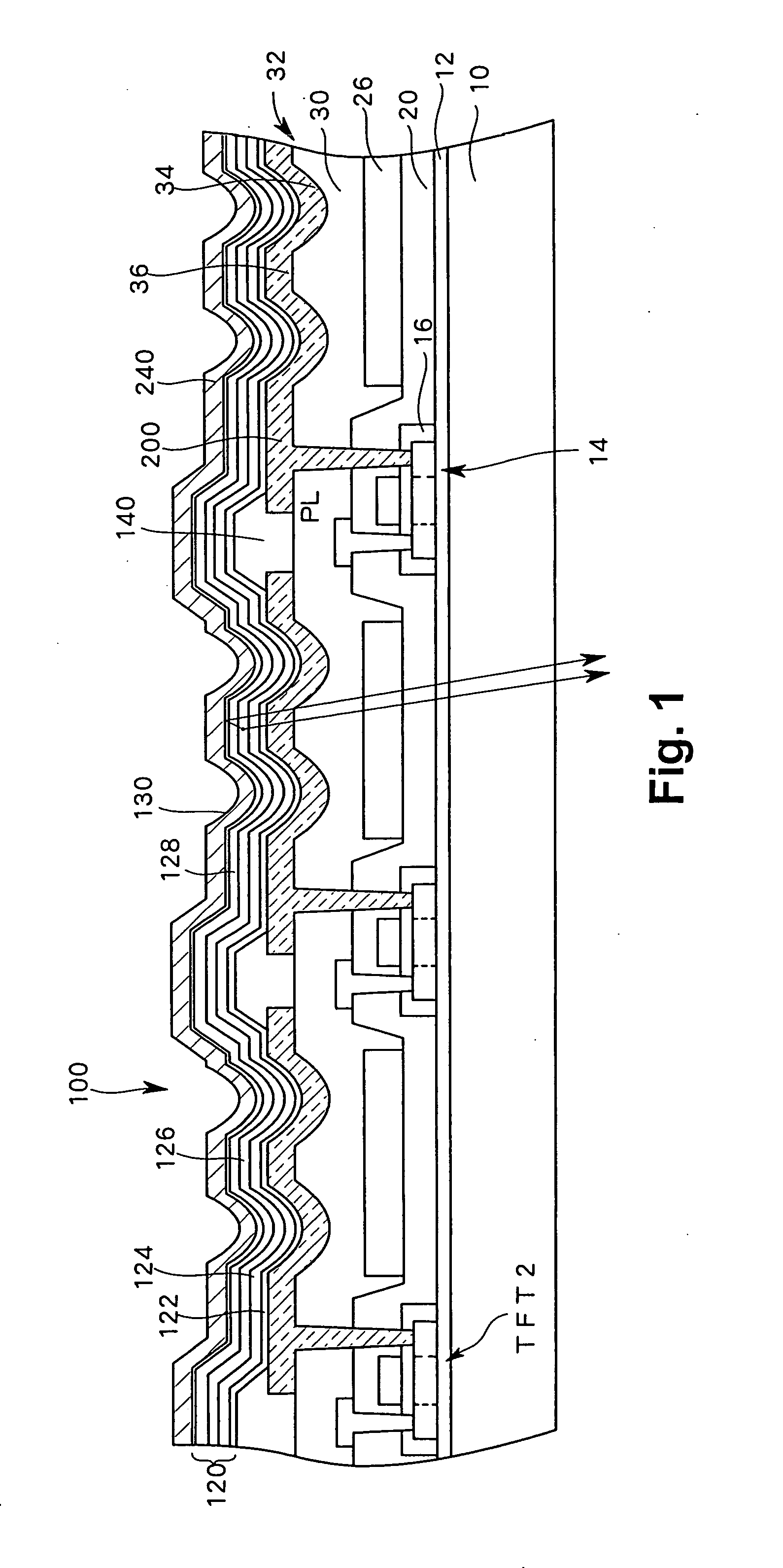
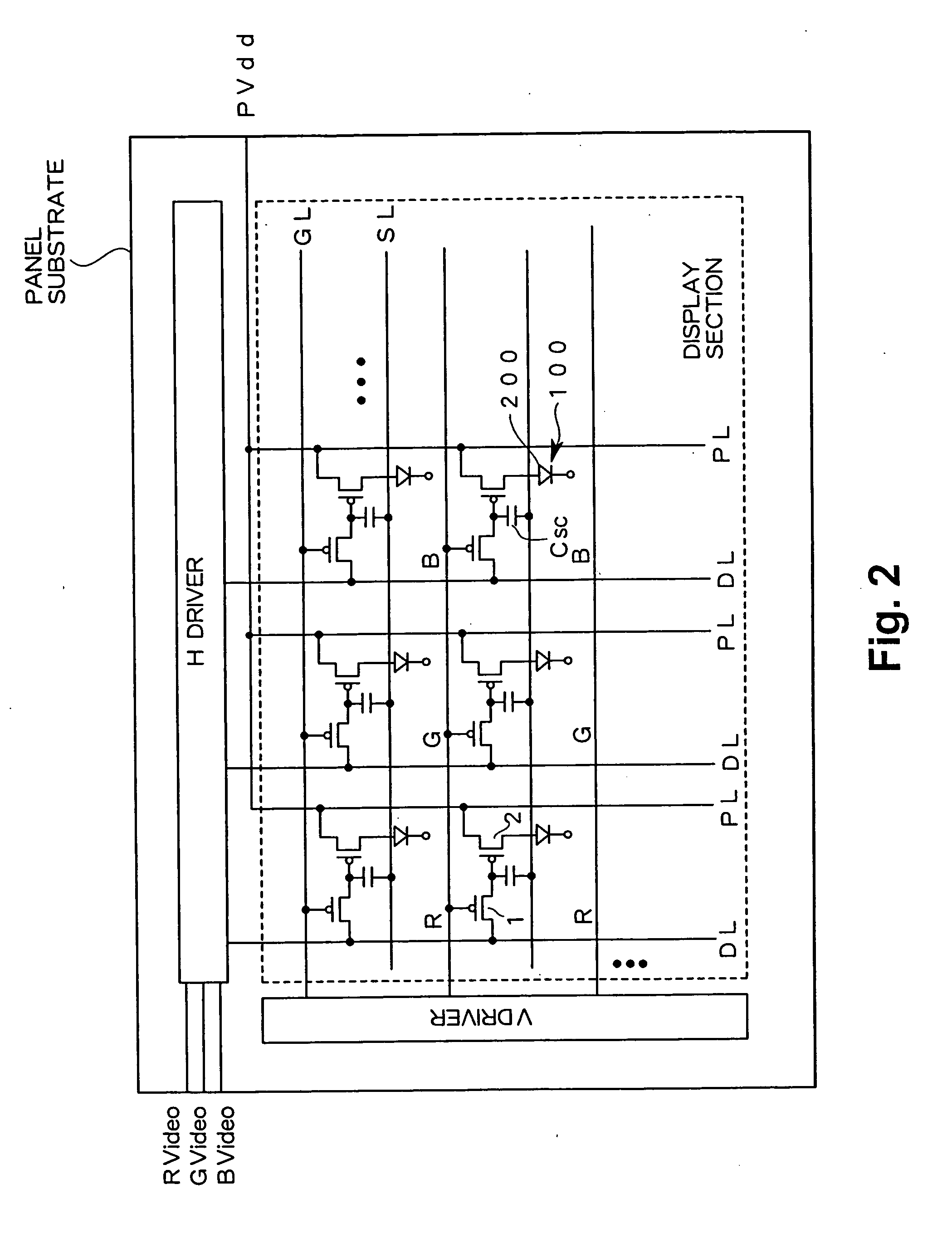
[0032]FIG. 1 schematically shows a cross sectional structure of an important part of a light emitting display device according to an embodiment of the present invention. FIG. 2 shows, as such a light emitting display device, an example of an equivalent circuit of an active matrix type display device having a thin film transistor (TFT) as a switch element controlling an emitting element for each pixel. As a light emitting display device, an organic EL display device using an organic EL element as an emitting element will be described hereinafter as an example.

[0033] In an active matrix type organic EL display device, a plurality of pixels are arranged in a matrix on a transparent substrate 10 formed of glass or the like, and each pixel includes, as illustrated in FIG. 2, an organic EL element 100, a first thin film transistor (hereina...


PUM


Abstract

Disclosed is a light-emitting display having a plurality of pixels wherein each pixel comprises a light-emitting device (100) having a light-emitting element layer which is formed between a first electrode and a second electrode and contains at least a light-emitting layer. An insulating layer (30) is formed between the light-emitting device (100) and a surface of a first or second substrate on the viewing side of the display, and the insulating layer (30) is provided with recesses and projections in at least one or more pixel regions, thereby forming an optical path length adjusting portion (32). By forming such an optical path length adjusting portion (32) in a pixel region, there is an increase in the interference conditions for the light emitted from the light-emitting device (100) to the outside, thereby averaging the interference.

Description

TECHNICAL FIELD [0001] The present invention relates to a light emitting display, and more particularly to a display including an emitting element for each pixel. BACKGROUND ART [0002] Flat panel displays (FPD) that can be manufactured in reduced size and thickness have been attracting attentions in recent years, and especially a liquid crystal display device, a typical type of the FPDs, has already been employed in a variety of equipments. At present, emissive devices (displays and light sources) using a self-emissive electroluminescence (hereinafter referred to as “EL”) element, particularly organic EL displays capable of emitting light at a high luminance in various colors depending on the organic compound material used, have been actively researched and developed. [0003] In contrast to liquid crystal display devices in which the transmission rate of light from a back light is controlled by a liquid crystal panel disposed on a front surface thereof as a light valve, such organic ...

Claims


Application Information

Patent Timeline
IPC IPC(8): G09G3/32H01L27/32H01L51/52H05B33/02H05B33/12H05B33/14
CPCH01L27/3213H01L27/322H01L27/3244H05B33/22H01L51/5262H01L51/5265H01L51/5209H10K59/351H10K59/38H10K59/124H10K50/813H10K50/85H10K50/852H10K2102/351
Inventor NISHIKAWA, RYUJIOMURA, TETSUJI
Owner SANYO ELECTRIC CO LTD
Why Eureka
Try Eureka