

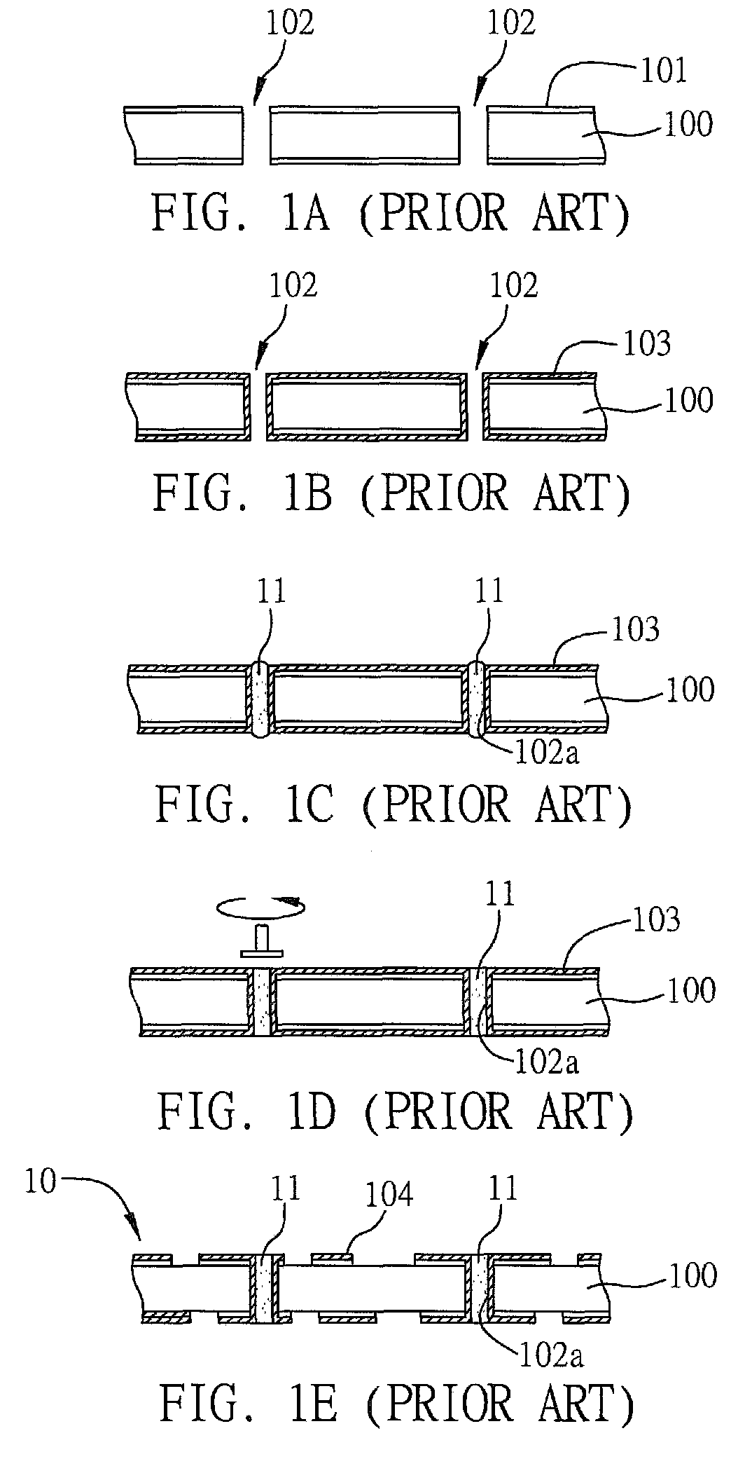
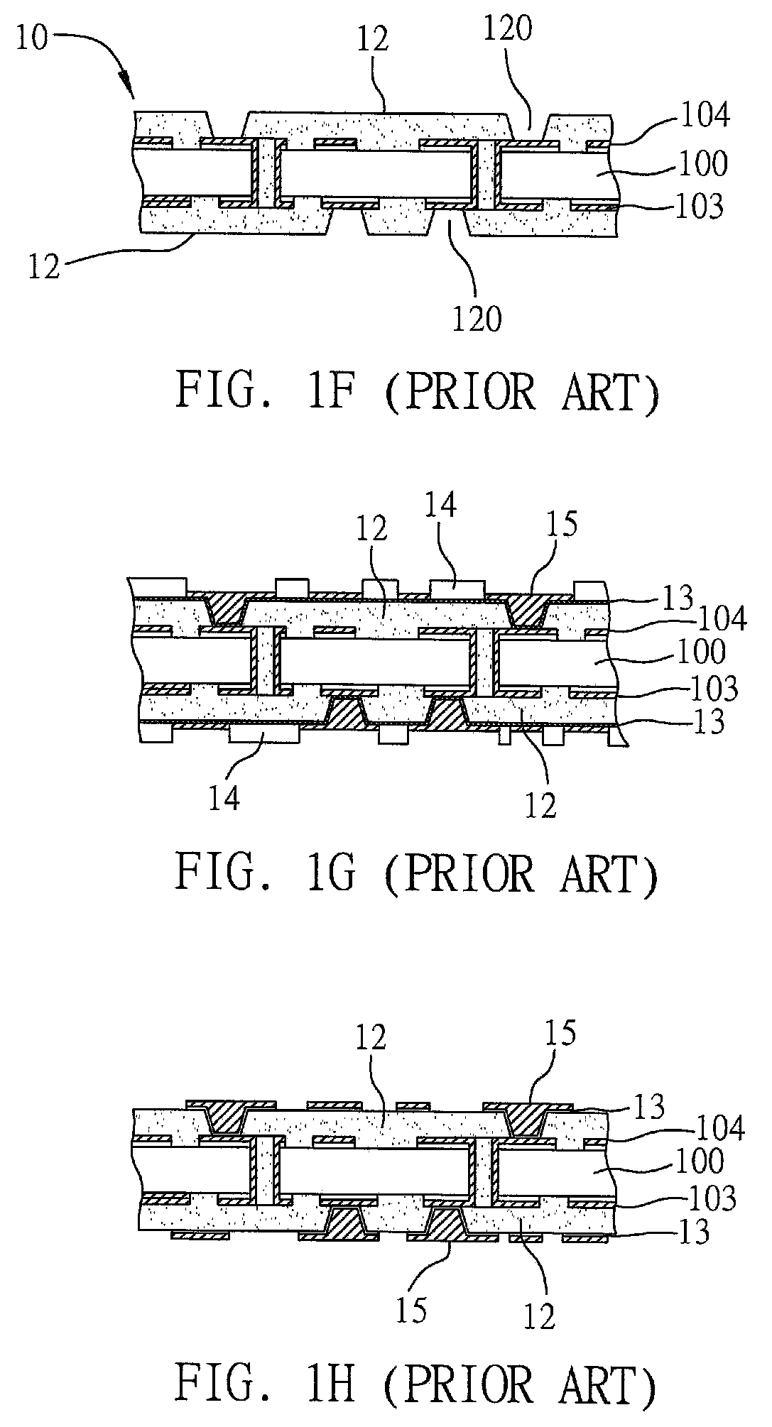
Structure of circuit board and method for fabricating same
a technology of circuit board and structure, applied in the direction of fixed capacitor details, fixed capacitors, fixed capacitor terminals, etc., can solve the problems of serious damage to the reduced production yield of circuit boards, and inability to reduce the thickness of finished multi-layer circuit boards, so as to reduce the size of package products, enhance electrical functionality, and reduce the effect of thickness
- Summary
- Abstract
- Description
- Claims
- Application Information
AI Technical Summary
Benefits of technology
Problems solved by technology
Method used
Image

Examples
first embodiment
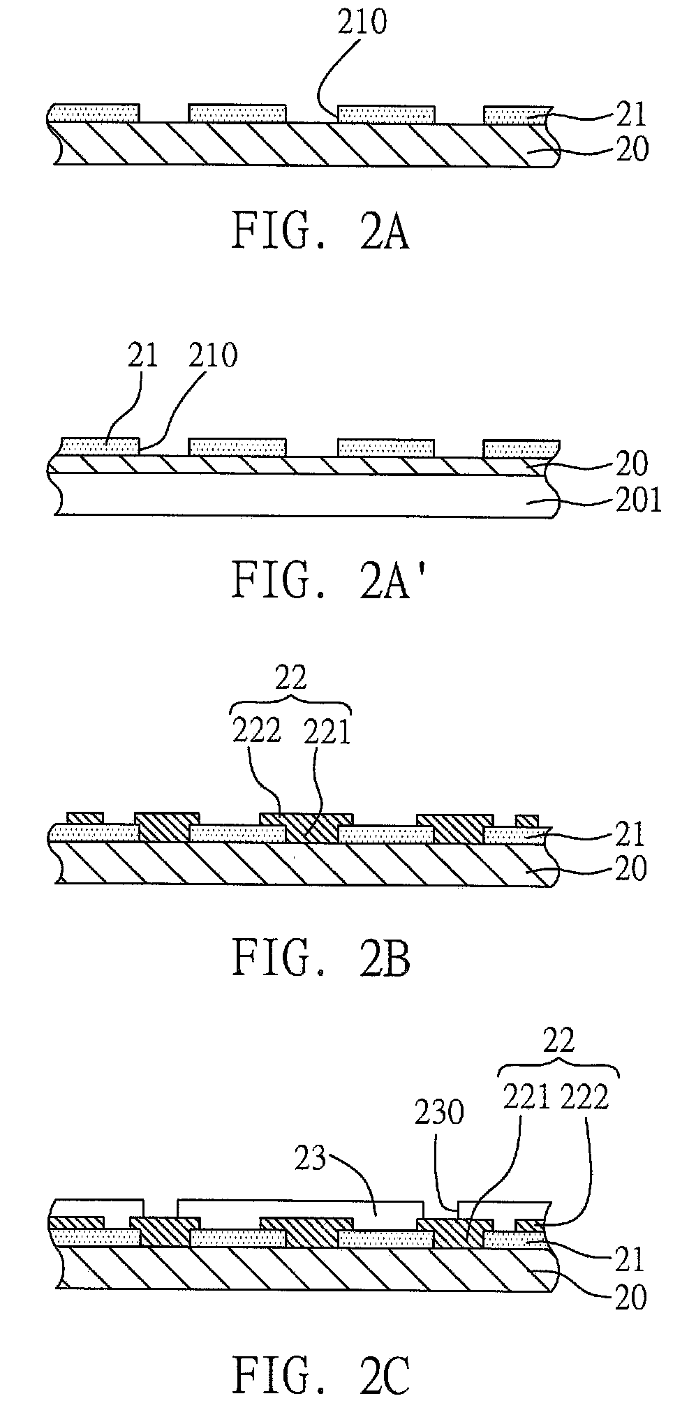
[0024]FIGS. 2A to 2F′ are cross-sectional views showing the method in accordance with the first embodiment of the present invention.
[0025]As shown in FIG. 2A, a carrier board 20 is provided at first; the carrier board 20 is made of metal, preferably of copper, but is not limited to it. Then an insulating protective layer 21 made of a photosensitive dielectric material or a solder mask layer is formed on the carrier board 20, and a plurality of openings 210 are formed in the insulating protective layer 21 to thereby expose parts of the carrier board 20.
[0026]As shown in FIG. 2B, the carrier board 20 serves as a conductive pathway for forming a circuit structure 22 by electroplating. At first, a seed layer (not shown) is formed on the surface of the insulating protective layer 21 and the openings 210 by electroless plating. Then, a metal layer (not shown) and conductive vias 221 are formed by electroplating. Lastly, a patterned circuit layer 222 is formed by photolithography and etchi...
second embodiment
[0033]FIGS. 3A to 3F′ are cross-sectional views showing the method of the present invention in accordance with the second embodiment. Unlike the first embodiment, the second embodiment discloses forming conductive vias 32 and a patterned circuit layer 33 in turn rather than at the same time.
[0034]As shown in FIG. 3A, the method further involves providing a carrier board 30 made of metal, forming an insulating protective layer 31 on the carrier board 30, forming a plurality of openings 310 in the insulating protective layer 31 to thereby expose the carrier board 30, and forming the conductive vias 32 in the openings 310 of the insulating protective layer 31.
[0035]As shown in FIG. 3B, the method further involves forming the patterned circuit layer 33 on top surfaces of the conductive vias 32 and on the insulating protective layer 31, and connecting electrically parts of the patterned circuit layer 33 to the conductive vias 32. Prior to forming the patterned circuit layer 33, a seed la...
PUM
| Property | Measurement | Unit |
|---|---|---|
| size | aaaaa | aaaaa |
| thickness | aaaaa | aaaaa |
| diameter | aaaaa | aaaaa |
Abstract
Description
Claims
Application Information