

Method for fabricating a cylinder-type capacitor utilizing a connected ring structure
a cylinder-type capacitor and connected ring technology, applied in the direction of capacitors, semiconductor devices, electrical equipment, etc., can solve the problems of reducing the distance between cylinder-type storage nodes in the formation process of cylinder-type capacitors, and difficulty in maintaining a sufficient surface area, so as to reduce the leaning of storage nodes
- Summary
- Abstract
- Description
- Claims
- Application Information
AI Technical Summary
Benefits of technology
Problems solved by technology
Method used
Image

Examples
first embodiment
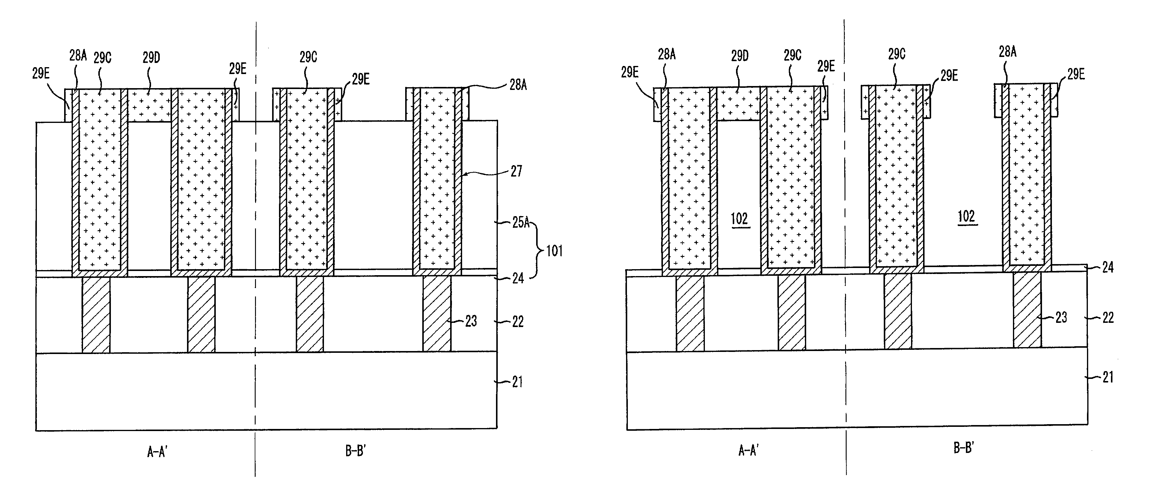
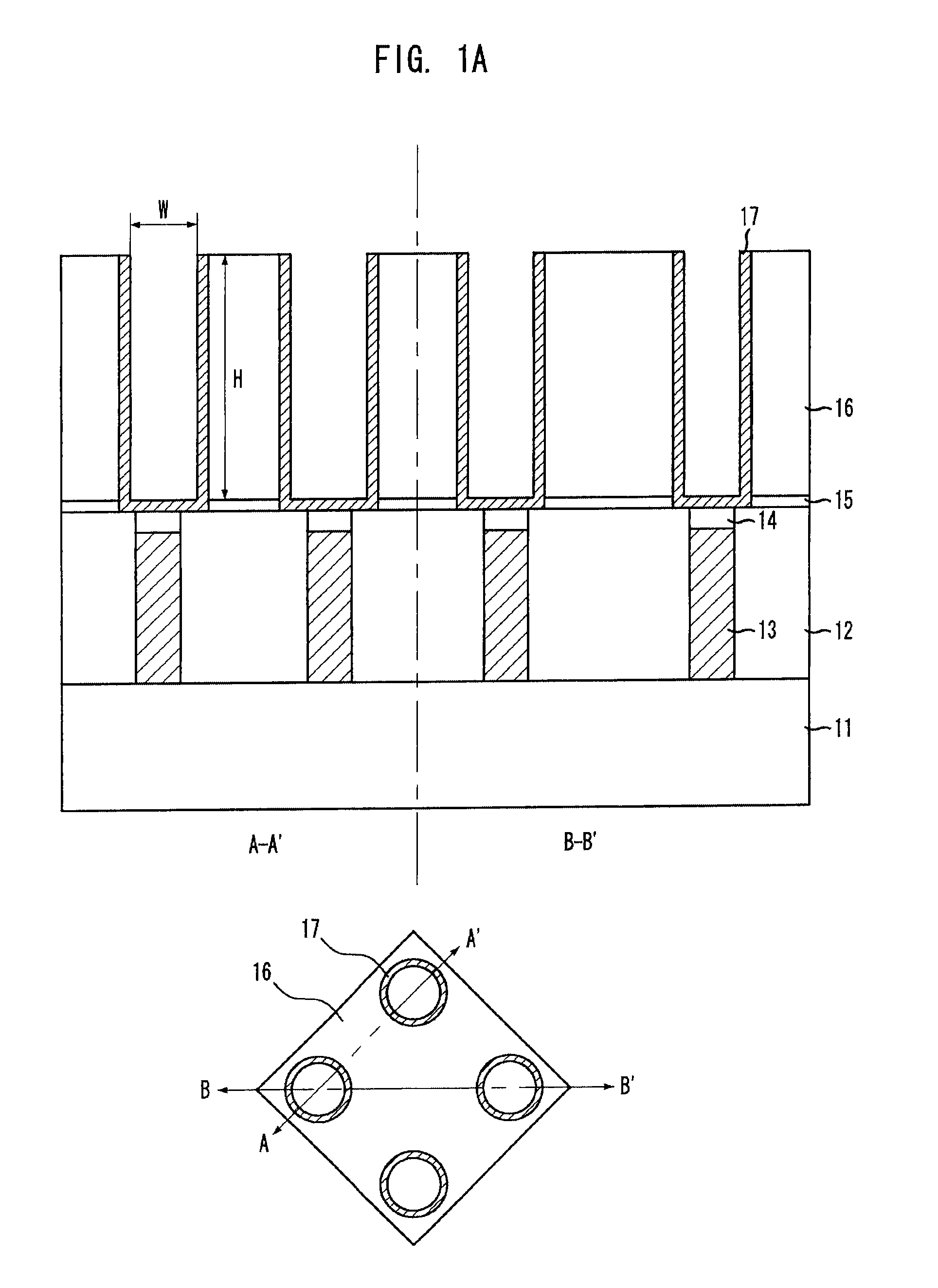
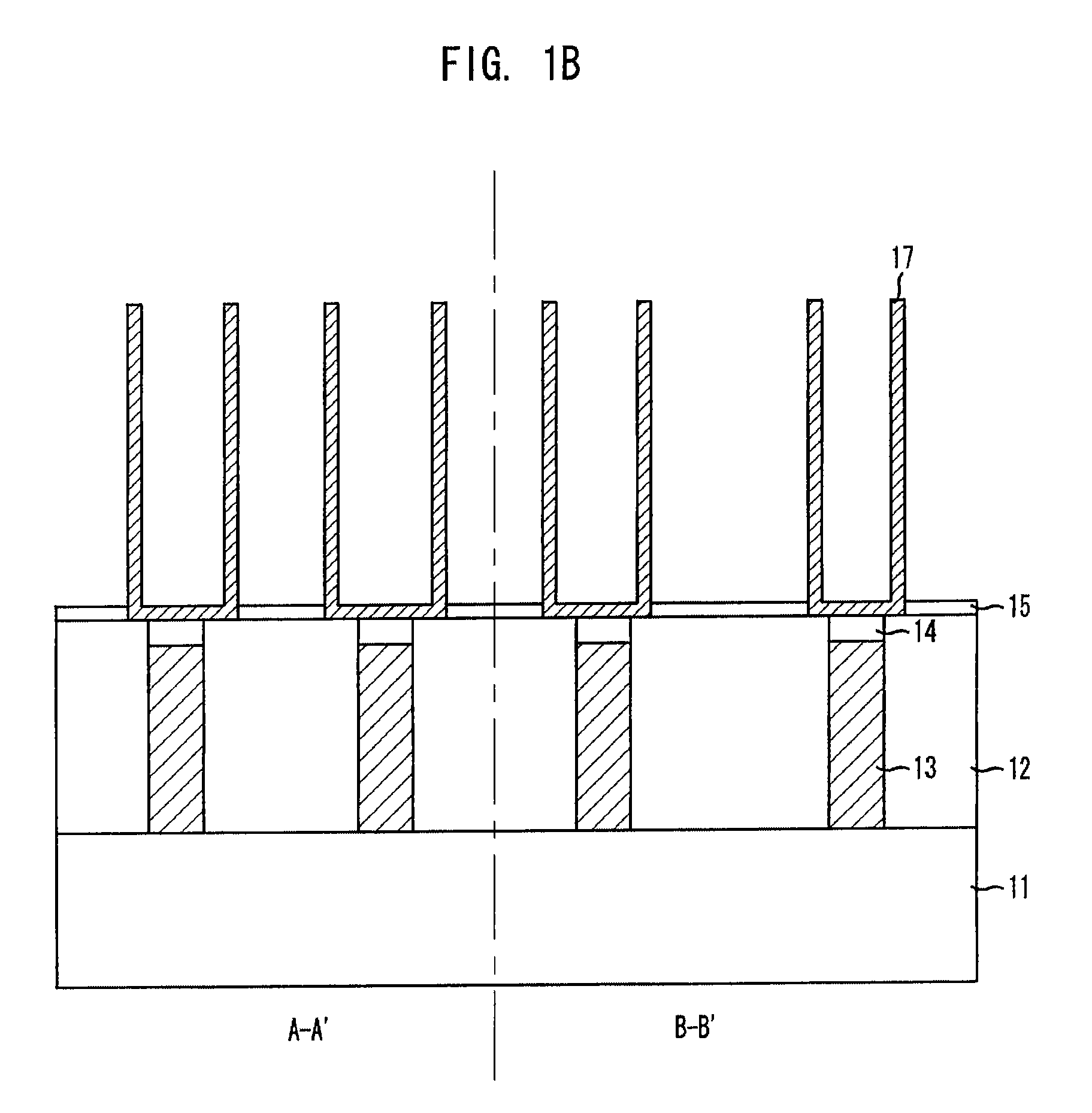
[0031]FIGS. 2A to 2H illustrate cross-sectional views of a method for fabricating a cylinder type capacitor according to the present invention. A line A-A′ represents a cross-sectional view of a substrate structure having a zigzag arrangement with a small spacing distance. A line B-B′ represents a cross-sectional view of the substrate structure having a zigzag arrangement with a large spacing distance.
[0032]Referring to FIG. 2A, an insulation layer 22 is formed over a semi-finished substrate 21. Storage node contact holes are formed in the insulation layer 22, and storage node contact plugs 23 are formed in the storage node contact holes. Although not illustrated, processes for forming transistors, word lines, and bit lines are generally performed before forming the insulation layer 22. The insulation layer 22 may include an undoped silicate glass (USG) layer and may be formed to have a thickness ranging from approximately 1,000 Å to approximately 3,000 Å. A patterned etch stop laye...
second embodiment
[0061]FIGS. 4A to 4H illustrate cross-sectional views of a method for fabricating a cylinder type capacitor according to the present invention.
[0062]Referring to FIG. 4A, an insulation layer 32 is formed over a semi-finished substrate 31. The substrate 31 is divided into a cell region and peripheral regions. Storage node contact holes are formed in the insulation layer 32, and storage node contact plugs 33 are formed in the storage node contact holes. Although not illustrated, processes for forming transistors, word lines, and bit lines are generally performed before forming the insulation layer 32. The insulation layer 32 may include an undoped silicate glass (USG) layer and may be formed to have a thickness ranging from approximately 1,000 Å to approximately 3,000 Å. A patterned etch stop layer 34 is formed over the insulation layer 32. A patterned mould layer 35 is formed over the patterned etch stop layer 34.
[0063]The insulation layer 32 is etched using a storage node contact ma...
third embodiment
[0082]FIGS. 5A to 5H illustrate cross-sectional views of a method for fabricating a cylinder type capacitor according to the present invention.
[0083]Referring to FIG. 5A, an insulation layer 42 is formed over a semi-finished substrate 41. The substrate 41 is divided into a cell region and peripheral regions. Storage node contact holes are formed in the insulation layer 42, and storage node contact plugs 43 are formed in the storage node contact holes. Although not illustrated, processes for forming transistors, word lines, and bit lines are generally performed before forming the insulation layer 42. The insulation layer 42 may include an undoped silicate glass (USG) layer and may be formed to have a thickness ranging from approximately 1,000 Å to approximately 3,000 Å. A patterned etch stop layer 44 is formed over the insulation layer 42. A patterned mould layer 45 is formed over the patterned etch stop layer 44.
[0084]The insulation layer 42 is etched using a storage node contact ma...
PUM
 Abstract
Description
Claims
Application Information