Method of fabricating semiconductor device having capacitor

a capacitor and semiconductor technology, applied in semiconductor devices, capacitors, electrical equipment, etc., can solve the problems of weak lower electrodes, high temperature of subsequent processes, and high cost, and achieve the effect of increasing capacitance and preventing the collapse or breakage of lower electrodes

Active Publication Date: 2005-03-15
SAMSUNG ELECTRONICS CO LTD
View PDF3 Cites 14 Cited by
  • Summary
  • Abstract
  • Description
  • Claims
  • Application Information

AI Technical Summary

Benefits of technology

Exemplary embodiments of the invention generally include methods for fabricating semiconductor devices having capacitors that provide increased capacitance and which prevent the collapse or breakage of lower electrodes of the capacitors.
In another exemplary embodiment of the invention, a method of fabricating a semiconductor device comprises: forming a first insulating layer on a semiconductor substrate; forming a contact hole in the first insulating layer; forming a contact plug with doped polysilicon in the contact hole; forming an etch stop layer on the contact plug and the first insulating layer; forming a second insulating layer on the etch stop layer; forming a storage node hole through the second insulating layer and the etch stop layer to expose the contact plug; selectively etching the exposed contact plug using a mixture of HBr and Cl2, and Ar plasma; forming a lower electrode on the selectively etched contact plug; and forming a capacitor by forming a dielectric layer and an upper electrode on the lower electrode. With this exemplary method, a portion from where the landing pad or contact plug is partially removed is used as a lower portion of the capacitor by forming the lower electrode after selectively etching the landing pad or the contact plug. Therefore, the capacitance of the capacitor can be increased. Furthermore, tilting of the lower electrode can be lessened due to enhanced support of the lower electrode by forming the lower electrode inside the landing pad or the contact plug.

Problems solved by technology

Among these conventional methods, the use of a material having a high dielectric constant requires time and money for introducing new equipment, verifying reliability, mass producing the dielectric layer, and lowering the temperature of subsequent processes.
In addition, with such structure, the lower electrode is likely to collapse due to the occurrence of surface tension when removing the mold oxide by wet etching after forming the lower electrode in the storage node hole and drying is performed.
Moreover, the weak lower electrode is likely to collapse or break due to thermal stress in subsequent processes.
Consequently, the resulting semiconductor device may malfunction due to the occurrence of bridges between cells.

Method used


Image

  • Method of fabricating semiconductor device having capacitor
  • Method of fabricating semiconductor device having capacitor
  • Method of fabricating semiconductor device having capacitor

Examples


Embodiment Construction

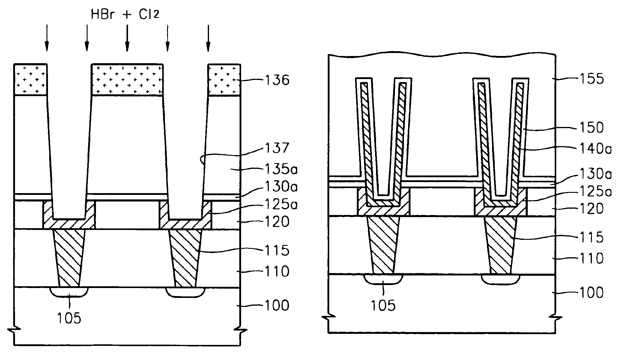
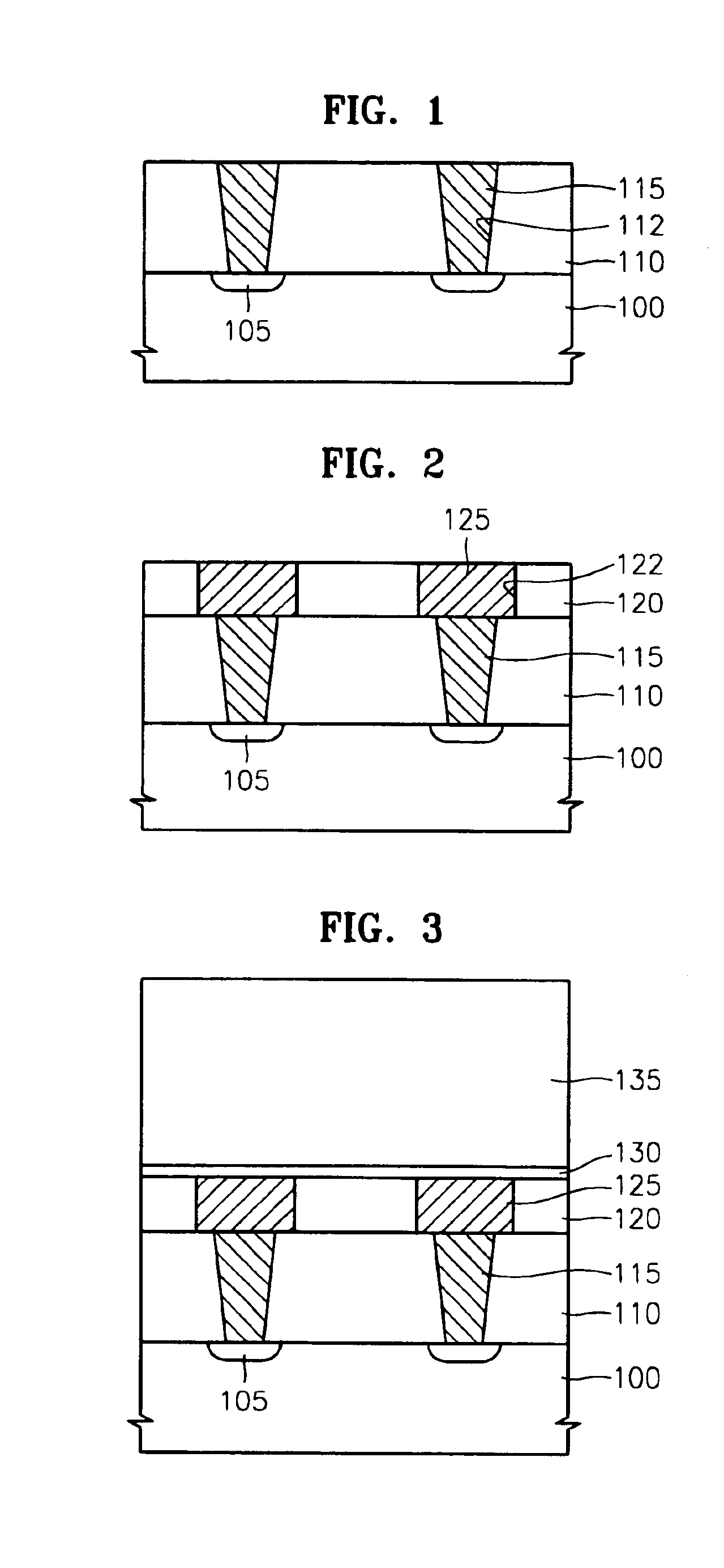
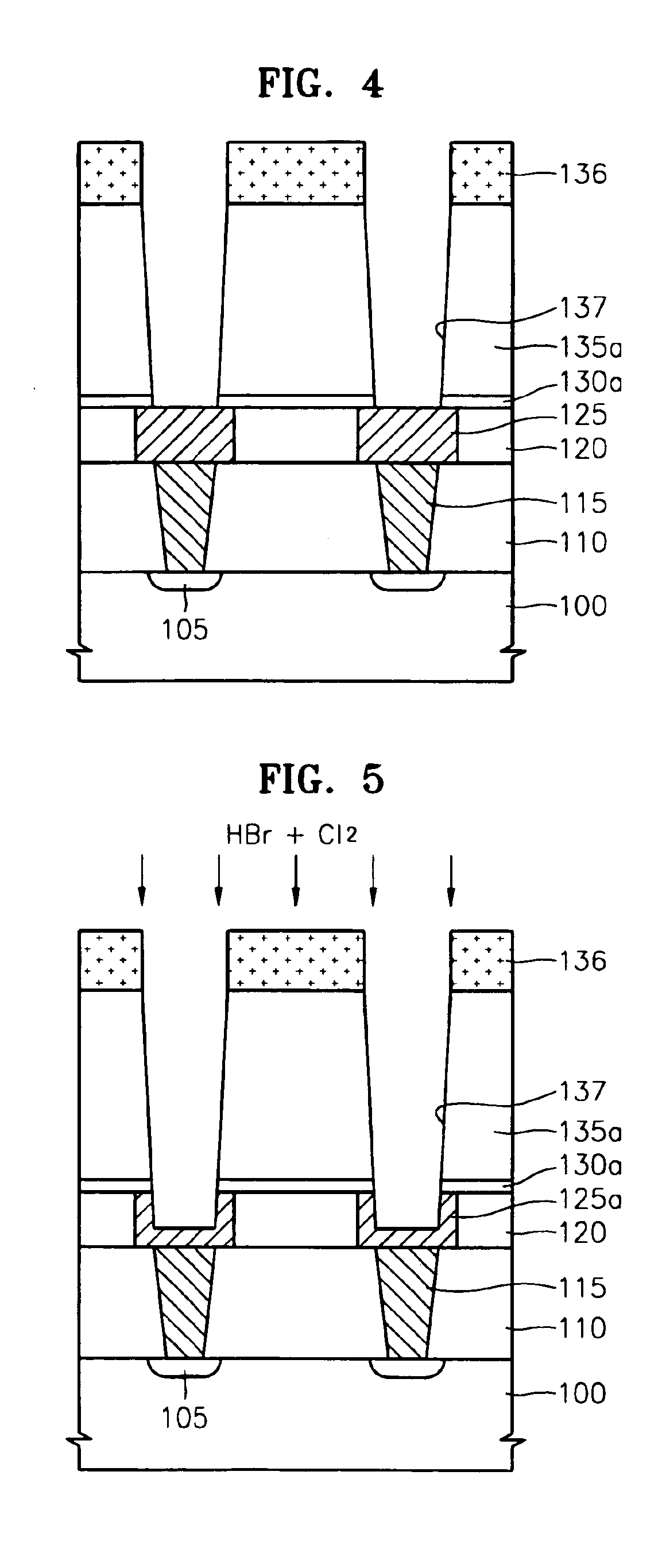
Hereinafter, exemplary embodiments of the present invention will be described more fully with reference to the accompanying drawings. These exemplary embodiments are provided so that this disclosure will be thorough and complete, and will fully convey concepts of the invention to one of ordinary skill in the art. However, one of ordinary skill in the art could readily envision other embodiments of the invention and nothing herein should be construed as limiting the scope of the invention. Further, it is to be understood that the drawings are schematic representations where the thickness of layers and regions are exaggerated for clarity. Moreover, the same reference numerals throughout the drawings may represent the same or similar elements, and thus their description may be omitted.

FIGS. 1 through 7 are schematic cross-sectional views illustrating a method for fabricating a semiconductor device according to an exemplary embodiment of the present invention. Referring initially to FIG...


PUM


Abstract

Methods are provided for fabricating semiconductor devices having capacitors, which prevent lower electrodes of the capacitors from breaking or collapsing and which provide increased capacitance of the capacitors. For instance, a method includes forming a first insulating layer on a semiconductor substrate, forming a first hole in the first insulating layer, forming a contact plug in the first hole, forming a second insulating layer having a landing pad, wherein the landing pad contacts an upper surface of the contact plug, forming an etch stop layer on the landing pad and the second insulating layer, forming a third insulating layer on the etch stop layer; forming a third hole through the third insulating layer and etch stop layer to expose the landing pad, selectively etching the exposed landing pad, forming a lower electrode on the selectively etched landing pad, and then forming a capacitor by forming a dielectric layer and an upper electrode on the lower electrode.

Description

CROSS-REFERENCE TO RELATED APPLICATIONThis application claims priority to Korean Patent Application No. 2003-41449, filed on Jun. 25, 2003, in the Korean Intellectual Property Office, the disclosure of which is fully incorporated herein by reference.TECHNICAL FIELD OF THE INVENTIONThe present invention relates to methods for fabricating semiconductor devices with capacitors having increased capacitance, and more particularly, to methods for fabricating capacitors, which prevent the collapse of lower capacitor electrodes and which provide increased capacitance.BACKGROUNDDue to a continual increase in the integration density of semiconductor devices such as dynamic random access memories (DRAMs), various methods have been considered for obtaining sufficient cell capacitance in a limited area. For example, methods for providing sufficient cell capacitance include, e.g., using a dielectric material having a high dielectric constant as a dielectric layer of a capacitor, reducing the thic...

Claims


Application Information

Patent Timeline
Patent Type & Authority Patents(United States)
IPC IPC(8): H01L21/02H01L21/3213H01L21/314H01L21/316H01L21/8242
CPCH01L28/91H01L21/32136H01L21/3142H01L21/31616H01L27/10855H01L21/31645H10B12/0335H10B99/00
Inventor CHO, SUNG-ILSON, SEUNG-YOUNGKANG, CHANG-JINCHI, KYEONG-KOOSHIN, JI-CHUL
Owner SAMSUNG ELECTRONICS CO LTD
Why Eureka
Try Eureka