Liquid crystal display device and method of fabricating the same

a technology of liquid crystal display and vertical electric field, which is applied in the direction of semiconductor devices, optics, instruments, etc., can solve the problems of increasing both cost and fabrication time, affecting the quality of display, and unable to achieve a wide viewing angle, so as to reduce product cost and fabrication time

Active Publication Date: 2011-04-05
LG DISPLAY CO LTD
View PDF15 Cites 3 Cited by
  • Summary
  • Abstract
  • Description
  • Claims
  • Application Information

AI Technical Summary

Benefits of technology

[0031]An advantage of the present invention is to provide a liquid crystal display device and method of fabricating the same that can reduce product cost and fabrication time.
[0032]Additional features and advantages of the present invention will be set forth in the description which follows, and in part will be apparent from the description, or may be learned by practice of the invention. These and other advantages of the invention will be realized and attained by the structure particularly pointed out in the written description and claims hereof as well as the appended drawings.
[0033]To achieve these and other advantages and in accordance with the purpose of the present invention, as embodied and broadly described herein, a liquid crystal display device includes an array substrate including: gate and data lines crossing each other to define a pixel region on a first substrate; a thin film transistor connected to the gate and data lines; and first and second height adjusters; an opposing substrate facing the array substrate; a liquid crystal layer between the array substrate and the opposing substrate; a gap spacer corresponding to the first height adjuster and contacting the array substrate and the opposing substrate; a first press-buffer spacer corresponding to the second height adjuster, contacting the opposing substrate and spaced apart from the array substrate; and a second press-buffer spacer contacting the opposing substrate and spaced apart form the array substrate, wherein a distance between the first press-buffer spacer and the array substrate is substantially less than a distance between the second press-buffer spacer and the array substrate.
[0034]In another aspect, a method of fabricating a liquid crystal display device includes: forming an array substrate including: forming a gate line and a gate electrode on a first substrate; forming a gate insulating layer on the gate line and the gate electrode; and forming a data line crossing the gate line to define a pixel region, a semiconductor layer and source and drain electrodes over the gate electrode, and first and second height adjusters, on the gate insulating layer; forming an opposing substrate facing the array substrate; forming a gap spacer and first and second press-buffer spacers contacting the opposing substrate, wherein the gap spacer corresponds to the first height adjuster and contacts the array substrate, the first press-buffer spacer corresponds to the second height adjuster, and a distance between the first press-buffer spacer and the array substrate is substantially less than a distance between the second press-buffer spacer and the array substrate; and interposing a liquid crystal layer between the array substrate and the opposing substrate.
[0035]In another aspect, a liquid crystal display device includes an array substrate including: gate and data lines crossing each other to define a pixel region; an opposing substrate facing the array substrate; a liquid crystal layer between the array substrate and the opposing substrate; a gap spacer contacting the array substrate and the opposing substrate; a first press-buffer spacer contacting one of the array substrate and the opposing substrate and spaced apart from the other of the array substrate and the opposing substrate; and a second press-buffer spacer contacting one of the array substrate and the opposing substrate and spaced apart from the other of the array substrate and the opposing substrate, wherein a distance between the first press-buffer spacer and the other of the array substrate and the opposing substrate spaced apart from the first press-buffer spacer is substantially less than a distance between the second press-buffer spacer and the other of the array substrate and the opposing substrate spaced apart from the second press-buffer spacer.

Problems solved by technology

The LCD device operated by the vertically induced electric field has a disadvantage in failing to achieve a wide viewing angle.
Accordingly, light leakage occurs, and thus display quality defects such as stains is caused.
However, as explained above, the related art IPS-LCD needs five mask processes, thus increasing both cost and fabrication time.

Method used


Image

  • Liquid crystal display device and method of fabricating the same
  • Liquid crystal display device and method of fabricating the same
  • Liquid crystal display device and method of fabricating the same

Examples


Embodiment Construction

[0046]Reference will now be made in detail to illustrated embodiments of the present invention, which are illustrated in the accompanying drawings.

[0047]FIG. 5 is a plan view illustrating an IPS-LCD device according to an embodiment of the present invention.

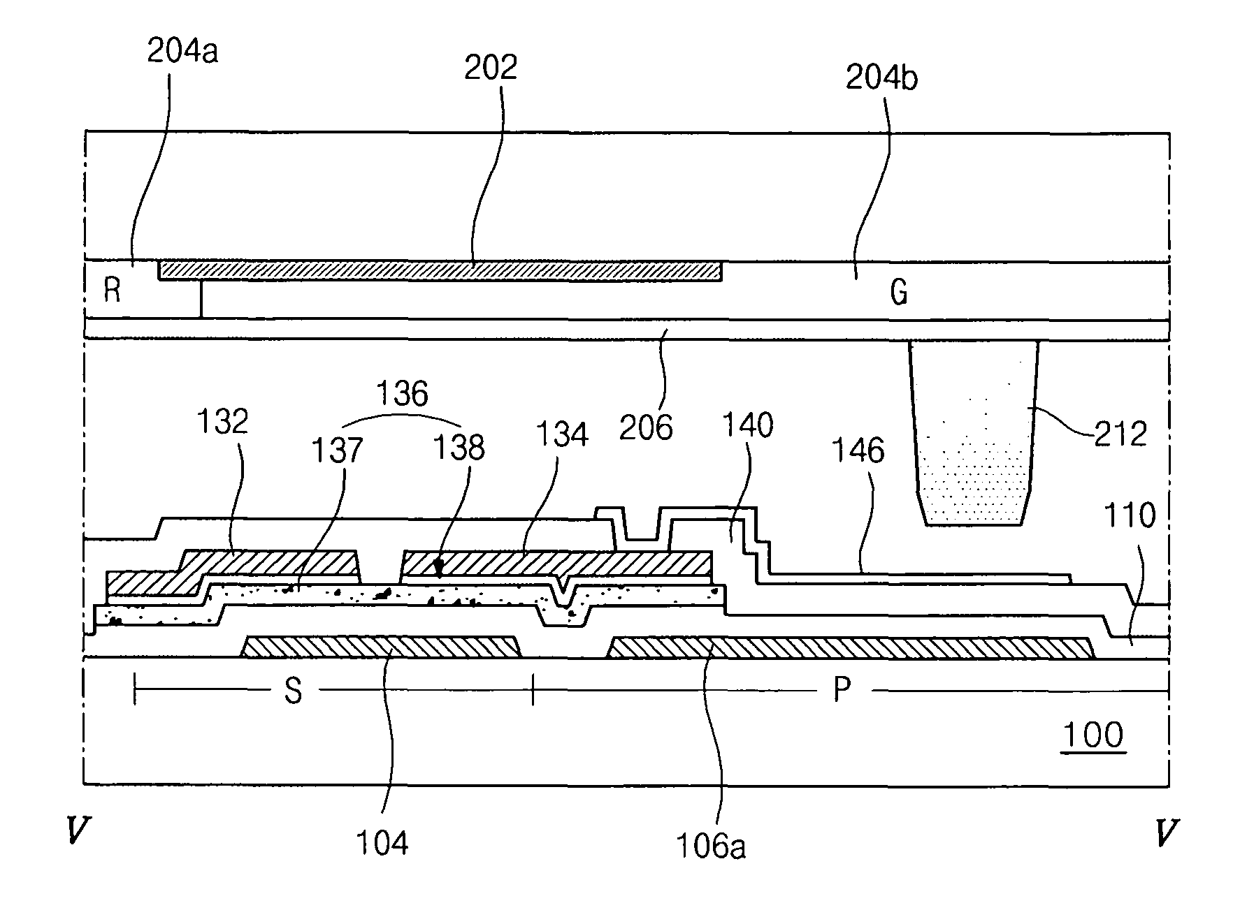
[0048]Referring to FIG. 5, in an array substrate of an IPS-LCD device according to an embodiment of the present invention, a gate line 102 and first and second common lines 106a and 106b extend along a first direction on a substrate 100. A data line 130 extends along a second direction crossing the first direction. A semiconductor pattern 122b below the data line 130 extends along the extension direction of the data line 130. The gate line 102 and the data line 130 define a pixel region P.

[0049]A thin film transistor T is located at a crossing portion of the gate and data lines 102 and 130. The thin film transistor T includes a gate electrode 104, a semiconductor layer 136 and source and drain electrodes 132 and 134. The semicond...


PUM

PropertyMeasurementUnit
thicknessesaaaaaaaaaa
thicknessaaaaaaaaaa
heightaaaaaaaaaa

Abstract

A liquid crystal display device includes an array substrate including: gate and data lines crossing each other to define a pixel region on a first substrate; a thin film transistor connected to the gate and data lines; and first and second height adjusters; an opposing substrate facing the array substrate; a liquid crystal layer between the array substrate and the opposing substrate; a gap spacer corresponding to the first height adjuster and contacting the array substrate and the opposing substrate; a first press-buffer spacer corresponding to the second height adjuster, contacting the opposing substrate and spaced apart from the array substrate; and a second press-buffer spacer contacting the opposing substrate and spaced apart form the array substrate, wherein a distance between the first press-buffer spacer and the array substrate is substantially less than a distance between the second press-buffer spacer and the array substrate.

Description

[0001]The present invention claims the benefit of Korean Patent Application No. 2006-0041835, filed in Korea on May 10, 2006, which is hereby incorporated by reference for all purposes as if fully set forth herein.BACKGROUND OF THE INVENTION[0002]1. Field of the Invention[0003]The present invention relates to a liquid crystal display device, and more particularly, to a liquid crystal display (LCD) device and a method of fabricating the same.[0004]2. Discussion of the Related Art[0005]Until recently, display devices have typically used cathode-ray tubes (CRTs). Presently, many efforts and studies are being made to develop various types of flat panel displays, such as liquid crystal display (LCD) devices, plasma display panels (PDPs), field emission displays, and electro-luminescence displays (ELDs), as a substitute for CRTs. Of these flat panel displays, LCD devices have many advantages, such as high resolution, light weight, thin profile, compact size, and low voltage power supply r...

Claims


Application Information

Patent Timeline
Patent Type & Authority Patents(United States)
IPC IPC(8): G02F1/1339
CPCG02F1/13394G02F1/1362H01L27/1288G02F1/136
Inventor KANG, DONG-HOSEO, YOUNG-ILCHO, SUNG-HYUN
Owner LG DISPLAY CO LTD
Why Eureka
Try Eureka