Liquid crystal display device

a display device and liquid crystal technology, applied in printed circuits, optics, instruments, etc., can solve the problems of increasing the physical size of the mold b>6/b>, the physical size of the display the physical size of the overall display device is more likely to occur, so as to reduce the physical size of the overall display device, increase the physical size of the display device, and enhance the reliability of connection

Active Publication Date: 2011-04-12
JAPAN DISPLAY INC +1
View PDF6 Cites 18 Cited by
  • Summary
  • Abstract
  • Description
  • Claims
  • Application Information

AI Technical Summary

Benefits of technology

[0027]The invention adopts the above means thereby achieving the reduction of physical size of the overall display device and enhancing the reliability of connection between the flexible wiring substrate and the liquid crystal display panel. The above means offer the following effects, respectively.
[0028]According to the means of the first to fifth aspects hereof, the recessed portion is formed at the portion where the terminals of the TFT substrate of the liquid crystal display panel are formed, and the flexible wiring substrate for supplying the signal from the external circuit, power and the like is connected via the recessed portion. The flexible wiring substrate is bent over the recessed portion toward the rear side of the liquid crystal display panel and hence, the flexible wiring substrate is accommodated in the recessed portion of the TFT substrate. This eliminates the problem that the flexible wiring substrate, which is bent, is protruded to outside so that the physical size of the display device is increased.
[0029]According to the means of the sixth to tenth aspects hereof, the recessed portion is formed at the portion where the terminals of the TFT substrate of the liquid crystal display panel are formed, and the flexible wiring substrate for supplying the signal from the external circuit, power and the like is connected via the recessed portion. The flexible wiring substrate is further extended toward the back side of the backlight disposed at place on the rear side of the liquid crystal display panel. The liquid crystal display panel and the backlight are accommodated in the mold. The recessed portion is formed at the terminal portion of the TFT substrate thereby allowing the flexible wiring substrate to be bent over the recessed portion toward the rear side. Therefore, the flexible wiring substrate is accommodated in the recessed portion of the TFT substrate so that the flexible wiring substrate may be accommodated in the mold. Consequently, the display device as a whole may be reduced in the physical size. Further, the flexible wiring substrate may encounter less chance to be subjected to the external force to separate the flexible wiring substrate from the terminal portion so that the reliability of the terminal connection is enhanced.
[0030]According to the means of the eleventh to fourteenth aspects hereof, the recessed portion is formed at the portion where the terminals of the TFT substrate of the liquid crystal display panel are formed, and the flexible wiring substrate for supplying the signal from the external circuit, power and the like is connected via the recessed portion. The flexible wiring substrate is further extended toward the back side of the backlight disposed at place on the rear side of the liquid crystal display panel. The liquid crystal display panel and the backlight are accommodated in the mold. Since the bottom of the mold is covered by the frame, it is easy to prevent the leakage of light from the light emitting diode as the light source of the backlight. Therefore, in addition to the effect to reduce the physical size of the display device as described with reference to the means of the sixth to tenth aspects hereof, the invention offers the effect to increase the use efficiency of the light from the backlight.
[0031]According the means of the fifteenth aspect in combination with the fourteenth aspect hereof, the use efficiency of the light from the backlight is further increased because the mold is housed in the frame. In addition, optical members of the backlight and the like may be retained in the frame in a stable manner.

Problems solved by technology

Such a problem is more likely to occur particularly before the mold 6 is housed in the frame 7.
Unfortunately however, the physical size of the mold 6 must be increased to allow the flexible wiring substrate 5 in the bent form to be installed therein.

Method used


Image

  • Liquid crystal display device
  • Liquid crystal display device
  • Liquid crystal display device

Examples


first embodiment

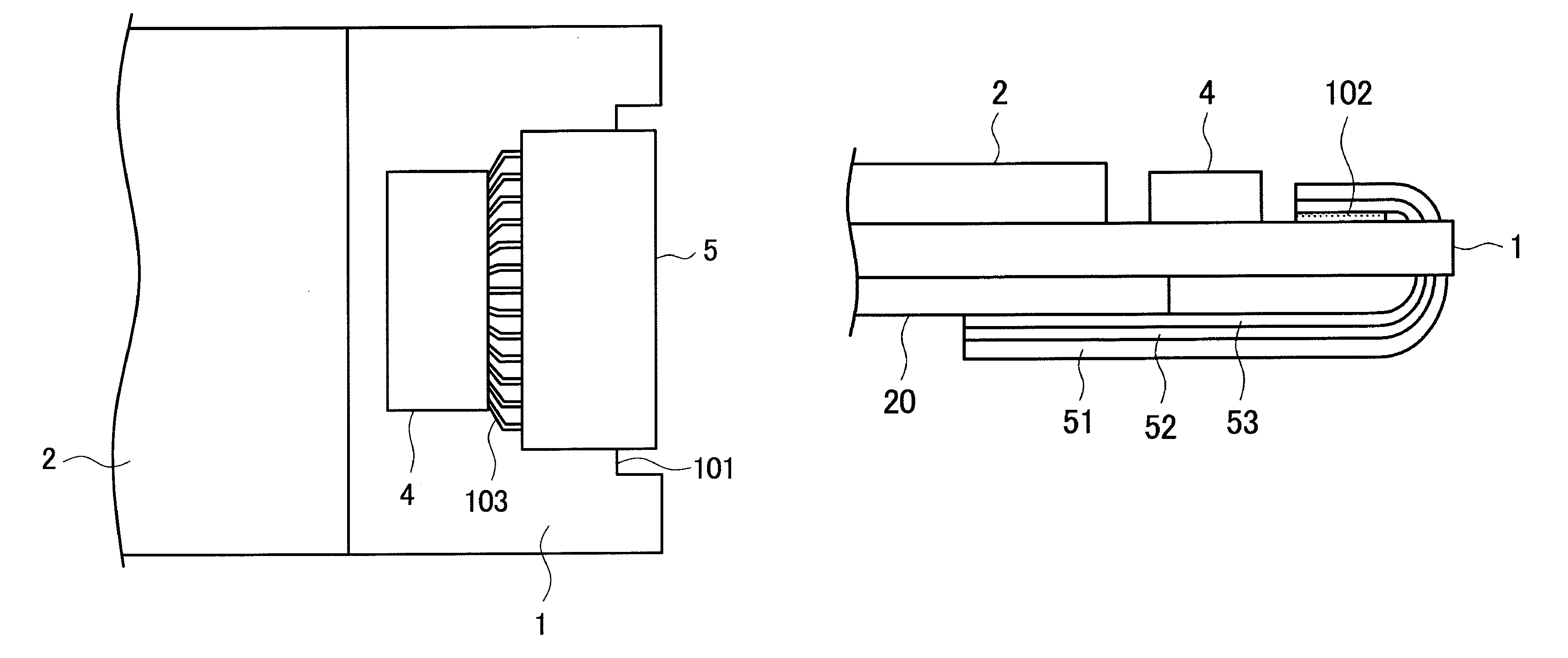
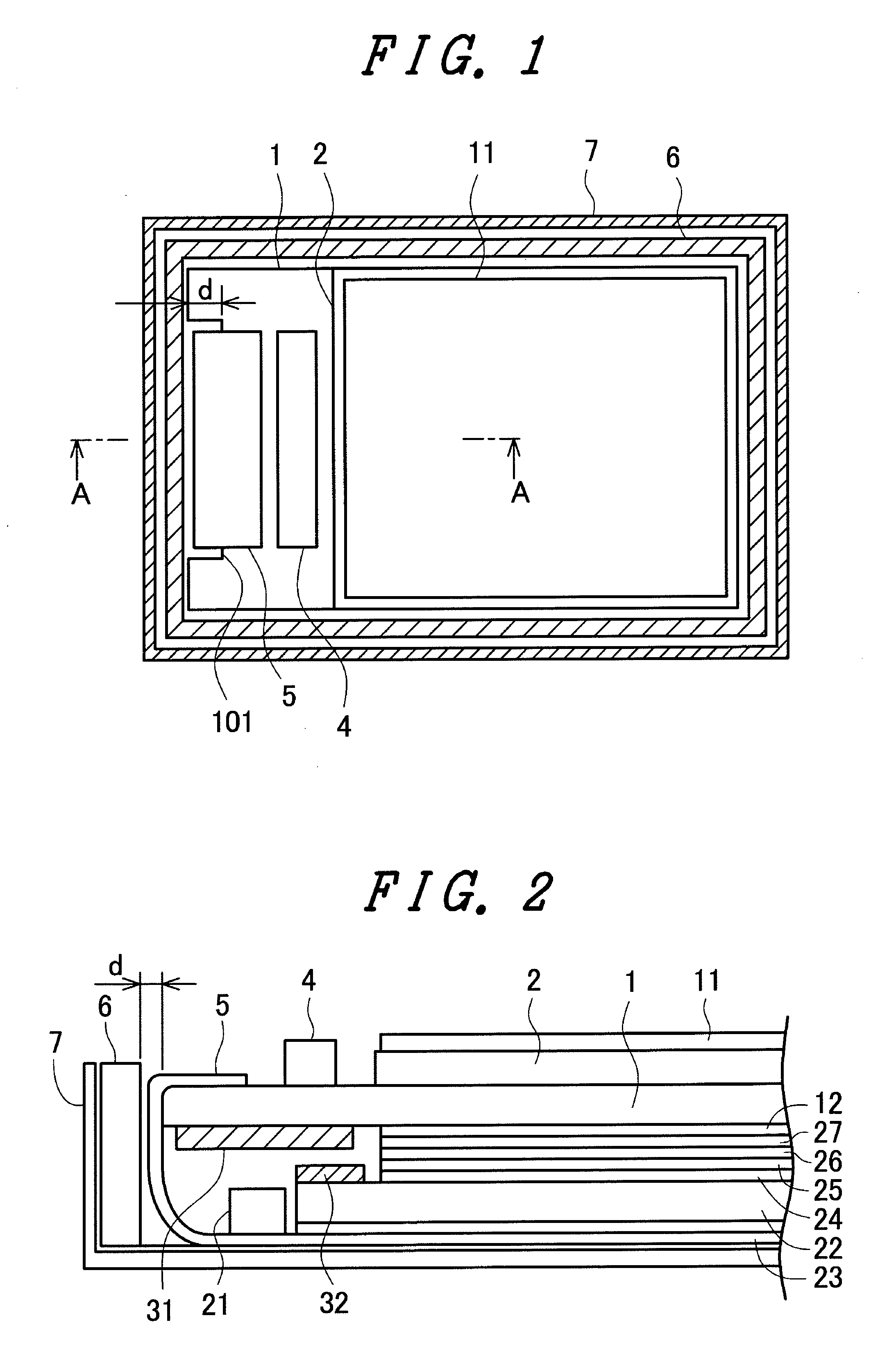
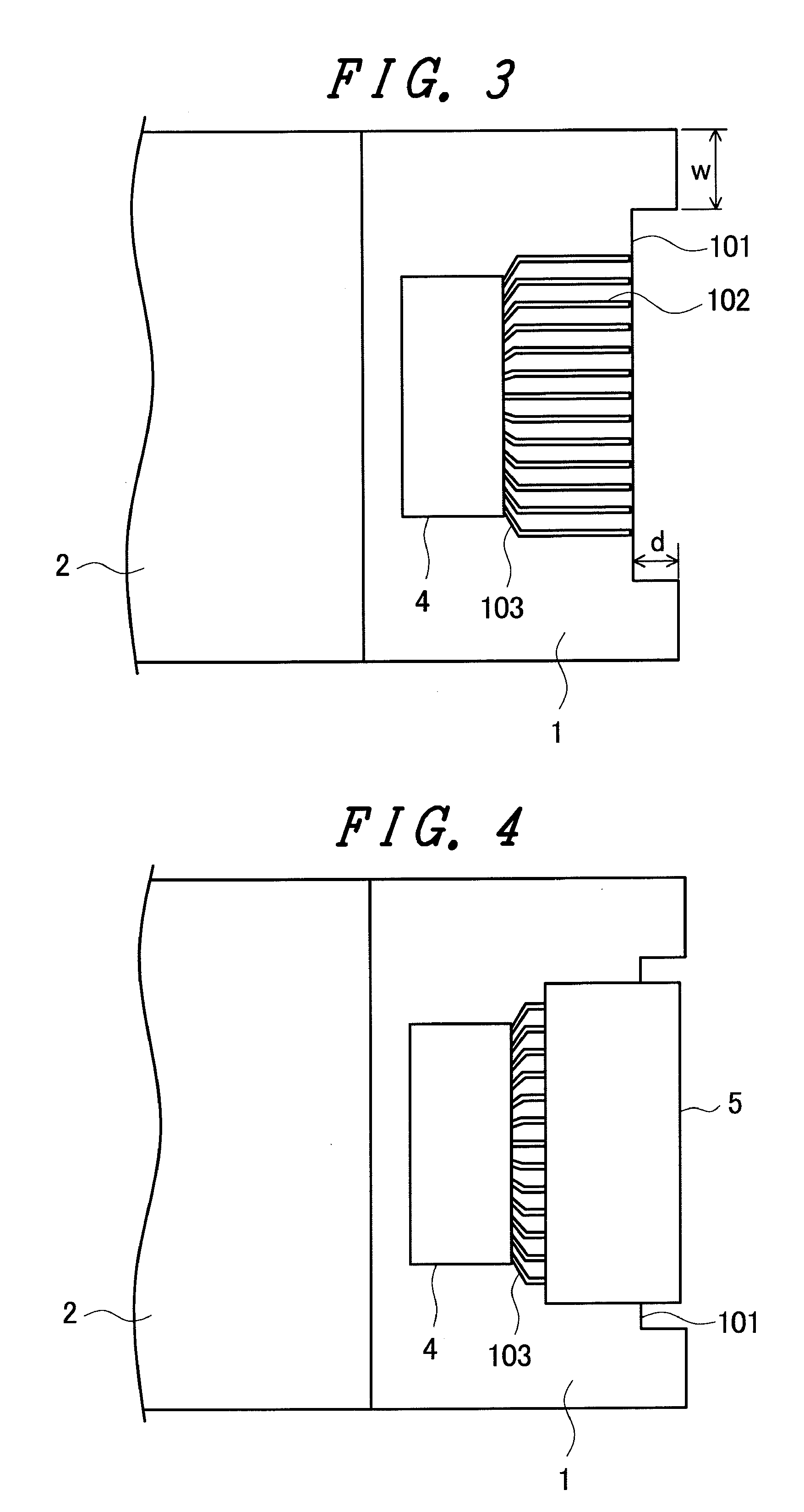
[0053]FIG. 1 is a plan view showing a first embodiment of the invention. FIG. 2 is a sectional view taken on the line A-A in FIG. 1. Referring to FIG. 1, a color filter substrate 2 of a liquid crystal display panel is disposed on a TFT substrate 1. The color filter substrate 2 has an upper polarizer 11 affixed to an upper side thereof. The upper polarizer 11 substantially corresponds to a viewing screen of the liquid crystal display panel. Mounted on one side of the TFT substrate 1 are a driving IC chip 4 for driving the liquid crystal display panel and a flexible wiring substrate 5 for connection with an external circuit.

[0054]The TFT substrate 1 is formed with a notch 101 at a portion where the flexible wiring substrate 5 is mounted. The depth of the notch 101 is represented as “d”. The thickness and bend allowance of the flexible wiring substrate 5 are accommodated by the notch 101. The flexible wiring substrate 5 is installed in a mold 6 as bent over toward a lower side of the l...

second embodiment

[0070]The first embodiment is arranged such that the mold 6 accommodating therein the liquid crystal display panel and the flexible wiring substrate 5 is housed in the metal frame 7. On the other hand, the invention is constituted such that the flexible wiring substrate 5 does not cover the mold 6 but is bent over toward the rear side as accommodated in the mold 6. This embodiment is designed to omit the metal frame 7 by utilizing the constitution of the invention. FIG. 11 is a schematic sectional view showing an arrangement of the second embodiment. The second embodiment potentially involves a fear of leakage of light from the LED 21 because a peripheral area of the LED is not covered by the frame 7.

[0071]This embodiment deals with this problem by adopting the following arrangement. As a first measure, a light shielding layer 33 or a light reflecting layer is formed on flexible wiring substrate 5 at an area surrounding the LED 21 thereby preventing the light from the LED 21 from le...

third embodiment

[0074]FIG. 13 illustrates a third embodiment of the invention. Referring to FIG. 13, the frame 7 is designed to be fitted on a lower part of the mold 6 rather than to house the whole body of the mold 6 therein. Unlike a conventional example, the mold 6 of the invention is not covered by the flexible wiring substrate 5 on an outside thereof. According to the invention, the flexible wiring substrate 5 is bent back as accommodated in the mold 6. Unlike the conventional example, therefore, the frame 7 does not play the role of accommodating therein the flexible wiring substrate 5 with respect to a planar direction of the display device. Accordingly, the embodiment may adopt the arrangement wherein the frame 7 is brought into engagement with a part of the mold 6, as shown in FIG. 13. Such an arrangement ensures that the frame 7 blocks off the peripheral area of the LED from outside so that the use efficiency of the light from the LED 21 may not be lowered. Since the frame 7 partially cov...


PUM

PropertyMeasurementUnit
depthaaaaaaaaaa
thicknessaaaaaaaaaa
thicknessaaaaaaaaaa

Abstract

An object of the invention is to reduce the size of a liquid crystal display device and to enhance the reliability of a connection portion with a flexible wiring substrate. According to the invention, liquid crystal is sandwiched between a TFT substrate and a color filter substrate. The TFT substrate is formed in a larger size than that of the color filter substrate. A connection portion with a flexible wiring substrate is formed on the TFT substrate. The TFT substrate is formed with a notch at its portion connected with the flexible wiring substrate. The flexible wiring substrate is bent over the notch toward a rear side of the liquid crystal display device as accommodated in a mold. This allows for the size reduction of the overall display device and ensures the enhanced reliability of the connection portion.

Description

CROSS-REFERENCE TO RELATED APPLICATIONS[0001]The disclosure of Japanese Patent Application No. 2006-310117 filed on Nov. 16, 2006 including the specification, drawings and abstract is incorporated herein by reference in its entirety.BACKGROUND[0002]1. Field of the Invention[0003]The present invention relates to a liquid crystal display device and particularly to a technique for reducing the physical size of a set and enhancing the reliability of a connection portion with an external circuit.[0004]2. Description of Related Arts[0005]The liquid crystal display devices have been faced with a strong demand to reduce the physical size of the unit while maintaining the same screen size. This demand is particularly strong in display devices, such as liquid crystal display device for use in cellular telephones, in which the reduction of the physical size of the unit is desired.[0006]FIG. 20 shows a structure of a module used in a conventional compact liquid crystal display device. FIG. 20A ...

Claims


Application Information

Patent Timeline
Patent Type & Authority Patents(United States)
IPC IPC(8): G02F1/1345G02F1/1333
CPCG02F1/13452H05K3/361G02F2001/133317H05K2201/09145H05K1/117G02F1/133317
Inventor ABE, HIDEAKI
Owner JAPAN DISPLAY INC
Why Eureka
Try Eureka