Additional aspects, features and advantages of the present invention are included in the following description of specific representative embodiments, which description should be taken in conjunction with the accompanying drawings.
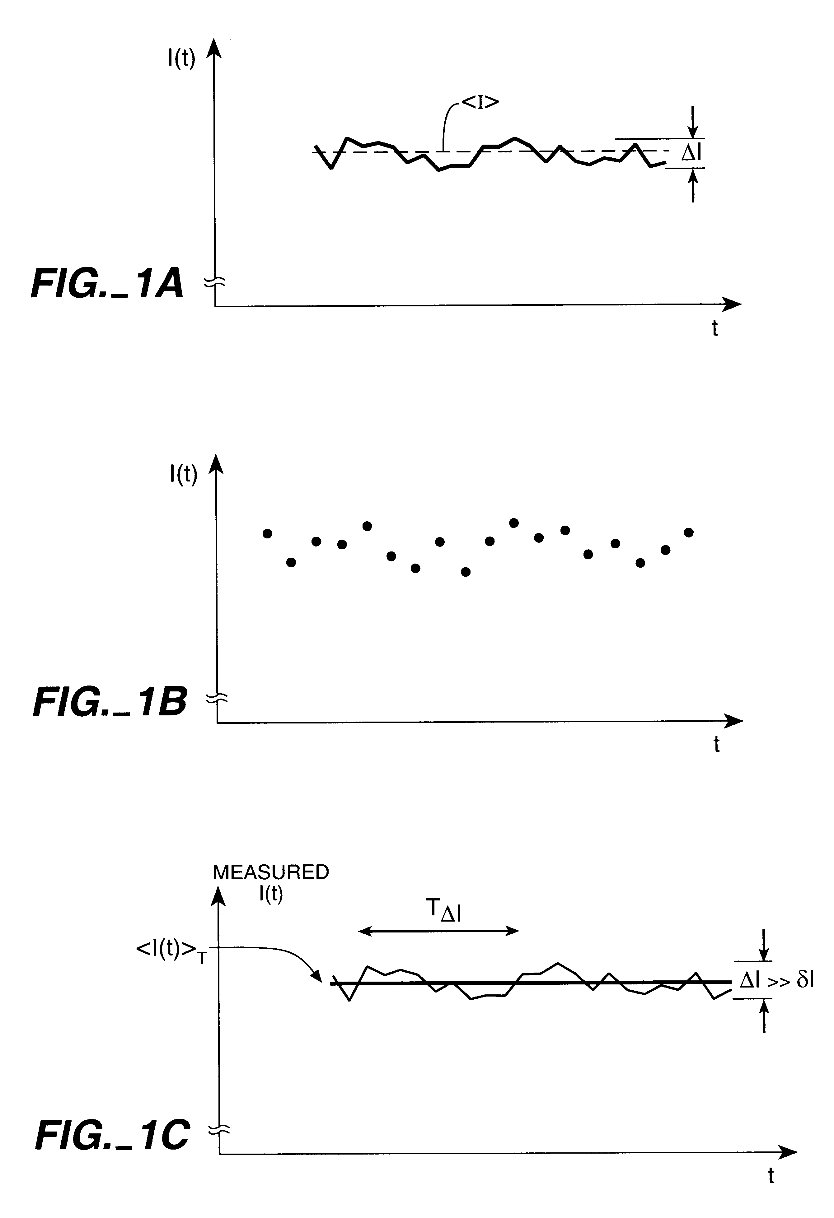
FIGS. 1A-C show examples of noisy response in a
memory cell.
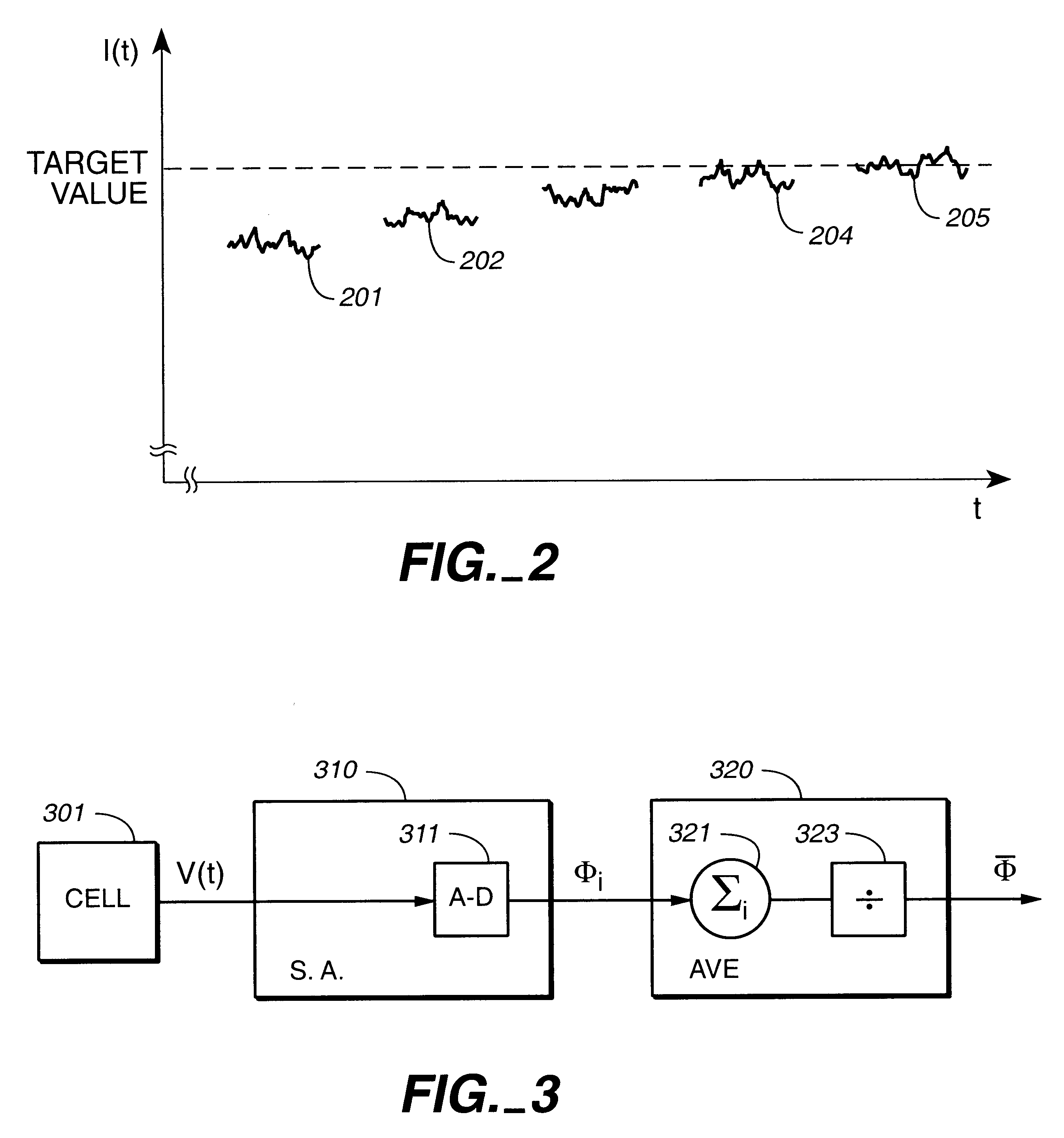
FIG. 2 illustrates the effect of noise on a program and verify operation.
FIG. 3 is a
schematic block diagram of the operation of the present invention according to an exemplary embodiment.
FIGS. 4A and 4B are block diagrams of circuit embodiments of some aspects of the present invention.
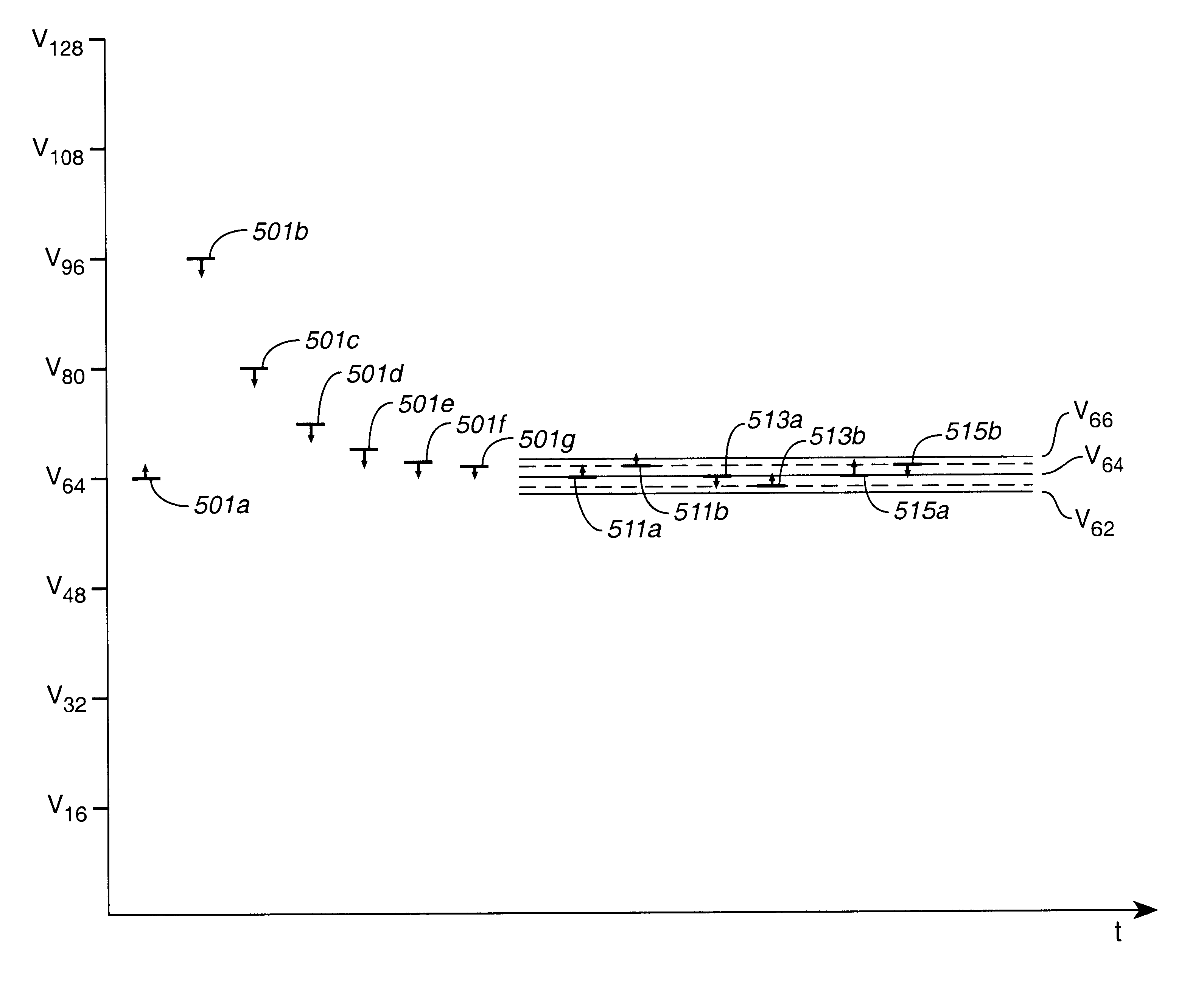
FIG. 5 is a
schematic representation of binary search implementation of an exemplary embodiment.
The storage capacity of non-volatile
semiconductor memories has increased both by the reduction in the physical size of the individual components of the circuits including the
memory cell and by increasing the amount of data storable in an individual memory
cell. For example, devices such as those described in U.S. Pat. Nos. 5,712,180 and 6,103,573 and U.S. patent applications Ser. No. 09 / 505,555, filed on Feb. 17, 2000, and Ser. No. 09 / 667,344, filed on Sep. 22, 2000, which are all assigned to SanDisk Corporation and which are all hereby incorporated herein by this reference, can store four or more logical bits per physical floating gate storage
transistor. In the case of four logical bits, this storage will require each floating gate to be able to have encoded within it one of sixteen possible memory states. Each one of these memory states corresponds to a unique value, or, more accurately, a
narrow range of values, of stored charge on the floating gate which is sufficiently separated from its neighboring states' charge storage range of values to clearly differentiate it from those neighboring states as well as all the other states. This is true for both a normal read operation as well as for a verify read done as part of a
programming operation.
A number of techniques for reading memory cells are described in U.S.
patent application Ser. No. 09 / 671,793, filed on Sep. 27, 2000, and one entitled "
Sense Amplifier for Multilevel Non-Volatile Integrated Memory Devices" by Shahzad Khalid, filed on Nov. 20, 2001, which are assigned to SanDisk Corporation and which are both hereby incorporated herein by this reference. The first of these applications describes reading the content of the memory cell with 7-bit or higher resolution for use in 4-bit storage. When this number of levels is contained in a 3
volt window of operating voltages as is typical in a
FLASH memory, this results in approximately a 25 mV resolving capability. With this range, levels of noise formerly acceptable can now lead to the state of the cell being read with an error of one or more state levels.
FIGS. 1A-C illustrate examples of noise fluctuations in the reading of a memory cell. FIG. 1A shows the case where the value of some parameter indicative of the state of the memory cell, in this case the current I(t) fluctuates around some mean value . In other embodiments, the memory can operate by reading voltage levels. If the value of the I(t) is read more or less instantaneously at regular intervals, the result would be something like what is shown in FIG. 1B. If instead the period over which the parameter indicating the state of the cell is read is several times longer than the typical time scale of the fluctuations, a relatively accurate value for the state of the cell can be determined. Some methods for accomplishing this are described in U.S. Pat. No. 6,044,019, from which FIGS. 1A and 1C are adapted and which has been incorporated by reference above.
As described in that patent, a memory cell has its source-
drain current I(t) sensed by a
sense amplifier. At the
sense amplifier, I(t) typically has a
noise component as illustrated in FIGS. 1A and 1C with noise fluctuations given by .
DELTA.I. One special feature of the
sense amplifier in that invention is to process this fluctuating current by means of an
integrator, which effectively produces a time-averaged current <I(t)>.sub.T over a predetermined period T. An A / D module further converts the sensed analog, time-averaged current into a digital format corresponding to an output memory state .PHI..
FIG. 1C illustrates a source-
drain current I(t) having noise fluctuations with a characteristic period T.sub..
DELTA.I, and the resulting time-averaged <I(t)>.sub.T as processed by the sense
amplifier of the present invention. The sensed source-
drain current of a memory cell, I(t) has a time-dependent
random noise component .
DELTA.I. When I(t) is averaged over a sufficient period of time T, the noise fluctuations are substantially attenuated. The
resultant error in <I(t)>.sub.T is given by .
delta.I which is substantially less than .DELTA.I. The sufficient period of time for averaging would be a period T substantially greater than a characteristic time T.sub..DELTA.I of the noise fluctuation. This T.sub..DELTA.I can be defined as a period where a predetermined amount of noise fluctuation has been sufficiently attenuated.
For example, in many
EEPROM or flash
EEPROM devices, the characteristic fluctuation time T.sub..DELTA.I has been estimated to be from 10 nanoseconds to several hundred nanoseconds. Thus, for these typical devices, the analog averaging or integration time T for the device described in U.S. Pat. No. 6,044,019 should preferably be substantially higher than T.sub..DELTA.I. In contrast, prior art sensing of I(t) is detected more or less "instantaneously", that is, in a time substantially less than T.sub..DELTA.I, and produces the sort of output shown in FIG. 1B depending on when the measurement is made. When the integration time T is essentially zero, as in the conventional case of no
time averaging, the noise fluctuation in a sensed current is given by .DELTA.I. As the averaging time is increased, the noise fluctuation in the time-averaged sensed current decreases due to increased phase cancellations.
Programming a memory cell is usually accomplished through a program / verify cycle, such as that described, for example, in U.S. Pat. No. 5,172,338 which is hereby incorporated by reference. In the typical process, a memory cell is pulsed with a programming voltage and its value is checked to determine whether or not it has reached the desired target state. If not, the process is then repeated until it is so verified. Since this
verification is a sensing process, it will also be affected by noise. This is shown in FIG. 2.
FIG. 2 shows the influence of noise on a program / verify process. After each programming pulse, the state of the cell is checked through a sensing process. Referring to FIG. 2, the state of the measured parameter, I(t), after such a pulse, is shown as the value I(t) 201 that includes a
noise component. As the state of the cell reflected by 201 is below the target value, the cell is again pulsed, as indicated by the blank interval, followed by a new sensing 202. As the state of the cell approaches the target value, the
noise component can lead to an erroneous
verification.
When the state of the cell is near the target value, the peaks in parameter due to noise may pass the target value, even through the cell is not yet in the desired state. This is shown by 204 where the peaks in I(t) cross the target value even though its average value, <I(t)>, is still not at the target value. If the verify read is performed at one of these peak values of 204, the cell could incorrectly verify instead of continuing on to the more accurate state represented by 205.

