Memory device with non-uniform programming levels

a memory device and programming level technology, applied in the field of memory devices, can solve the problem of non-uniform threshold voltage distribution of the device, and achieve the effect of reducing the spacing

Inactive Publication Date: 2011-04-12
APPLE INC
View PDF422 Cites 66 Cited by
  • Summary
  • Abstract
  • Description
  • Claims
  • Application Information

AI Technical Summary

Benefits of technology

[0016]In another embodiment, when one of the bit-specific error rates is to be increased with respect to the other bit-specific error rates in order to meet the condition, modifying the nominal storage values includes identifying a pair of the programming levels, such

Problems solved by technology

The threshold voltage distributions of the device are non-uniform and are designed to account for various impai

Method used


Image

  • Memory device with non-uniform programming levels
  • Memory device with non-uniform programming levels
  • Memory device with non-uniform programming levels

Examples


Embodiment Construction

Overview

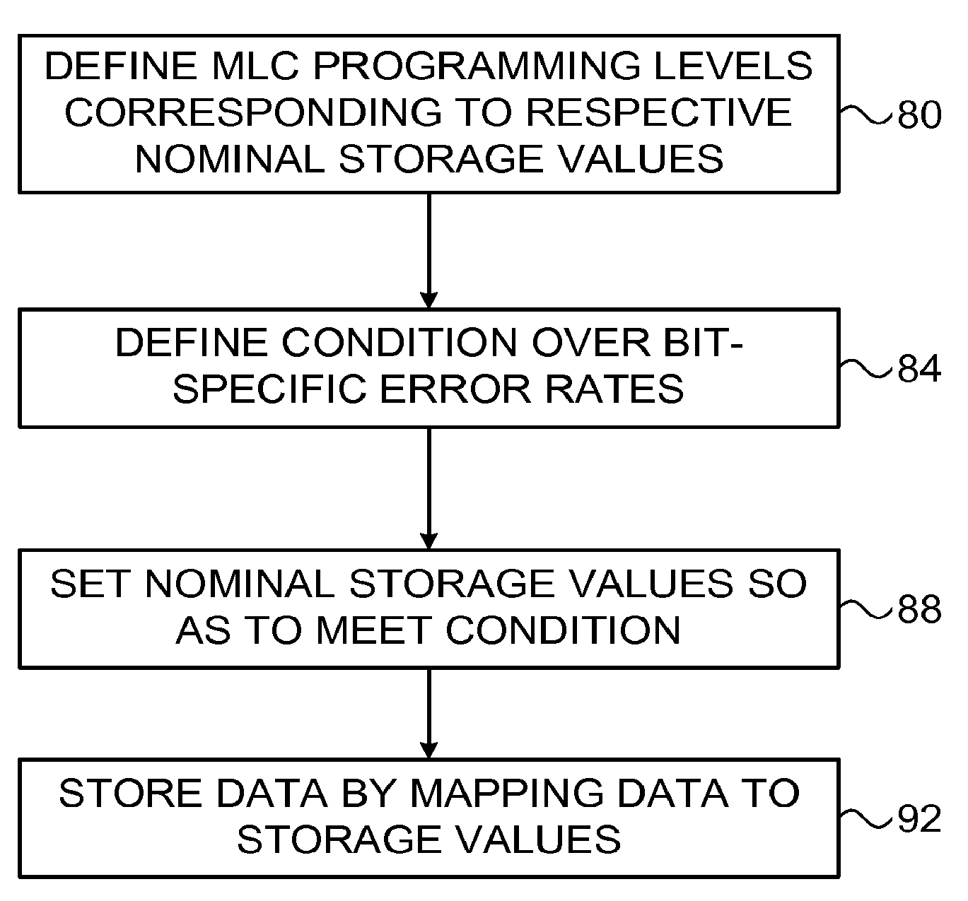
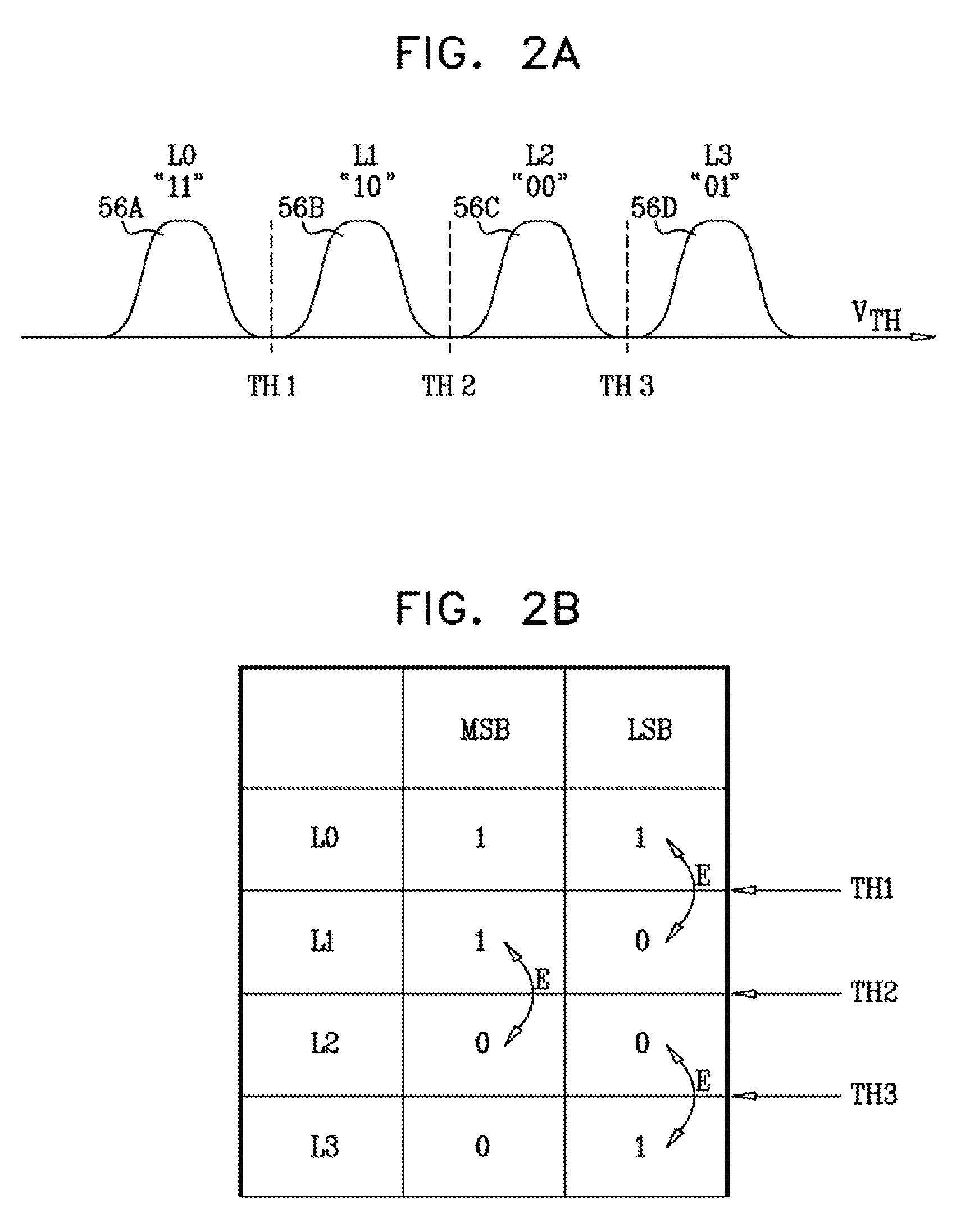
[0038]In a typical MLC configuration, each memory cell stores two or more data bits, and the cells are read by comparing their threshold voltages to a set of reference levels. A read error occurs when the threshold voltage of a given cell falls on the wrong side of a reference level and is therefore associated with the wrong programming level. Read errors are most likely to occur between adjacent programming levels. When the assignment of bit values to programming levels uses “Gray coding,” each read error between adjacent levels affects only a single bit.

[0039]Since the number of possible error events that affect each bit may not be the same for each MLC bit, different bits may have different Bit Error Rates (BERs). In some memory configurations, different MLC bits may be mapped to different memory pages, and therefore different pages may have different BERs. Uneven BER is often undesirable, for example because it increases the maximum possible number of errors per page. Wh...


PUM


Abstract

A method for storing data in a memory, which includes a plurality of analog memory cells, includes defining programming levels that represent respective combinations of at least first and second bits and are represented by respective nominal storage values. The data is stored by mapping the data to storage values selected from among the nominal storage values and writing the storage values to the memory cells. A condition is defined over two or more bit-specific error rates applicable respectively to at least the first and second bits. The bit-specific error rates include a first bit-specific error rate computed over the data stored by the first bits and a second bit-specific error rate computed, separately from the first bit-specific error rate, over the data stored by the second bits. The nominal storage values are set based on the bit-specific error rates so as to meet the condition.

Description

CROSS-REFERENCE TO RELATED APPLICATIONS[0001]This application claims the benefit of U.S. Provisional Patent Application 60 / 949,515, filed Jul. 13, 2007 and U.S. Provisional Patent Application 61 / 022,343, filed Jan. 20, 2008, whose disclosures are incorporated herein by reference.FIELD OF THE INVENTION[0002]The present invention relates generally to memory devices, and particularly to memory devices having non-uniform programming levels.BACKGROUND OF THE INVENTION[0003]Several types of memory devices, such as Flash memories, use arrays of analog memory cells for storing data. Each analog memory cell stores a quantity of an analog value, also referred to as a storage value, such as an electrical charge or voltage. The storage value represents the information stored in the cell. In Flash memories, for example, each analog memory cell holds a certain amount of electrical charge. The range of possible analog values is typically divided into regions, each region corresponding to one or mo...

Claims


Application Information

Patent Timeline
IPC IPC(8): G06F11/00G11C29/00
CPCG11C11/5628G06F11/1048
Inventor SOMMER, NAFTALI
Owner APPLE INC
Why Eureka
Try Eureka