System and method of generating hierarchical block-level timing constraints from chip-level timing constraints

a technology of hierarchical block and timing constraints, applied in computer aided design, program control, instruments, etc., can solve the problems of large and complex integrated circuits, millions of components, and time-consuming design of integrated circuits

Active Publication Date: 2011-04-12
CADENCE DESIGN SYST INC
View PDF10 Cites 13 Cited by
  • Summary
  • Abstract
  • Description
  • Claims
  • Application Information

AI Technical Summary

Problems solved by technology

Integrated circuits have become extremely large and complex, typically including millions of components.
It follows then that the design of integrated circuits is also very complex and time consuming, involving synthesizing, analyzing and optimizing many circuit parameters.
In many cases, an integrated circuit under development may be so complex that even EDA systems have difficulties in achieving design closure within a reasonable time period.

Method used


Image

  • System and method of generating hierarchical block-level timing constraints from chip-level timing constraints
  • System and method of generating hierarchical block-level timing constraints from chip-level timing constraints
  • System and method of generating hierarchical block-level timing constraints from chip-level timing constraints

Examples


Embodiment Construction

[0014]In the following detailed description of the embodiments of the invention, numerous specific details are set forth in order to provide a thorough understanding of the present invention. However, it will be obvious to one skilled in the art that the embodiments of the invention may be practiced without these specific details. In other instances well known methods, procedures, components, and circuits have not been described in detail so as not to unnecessarily obscure aspects of the embodiments of the invention.

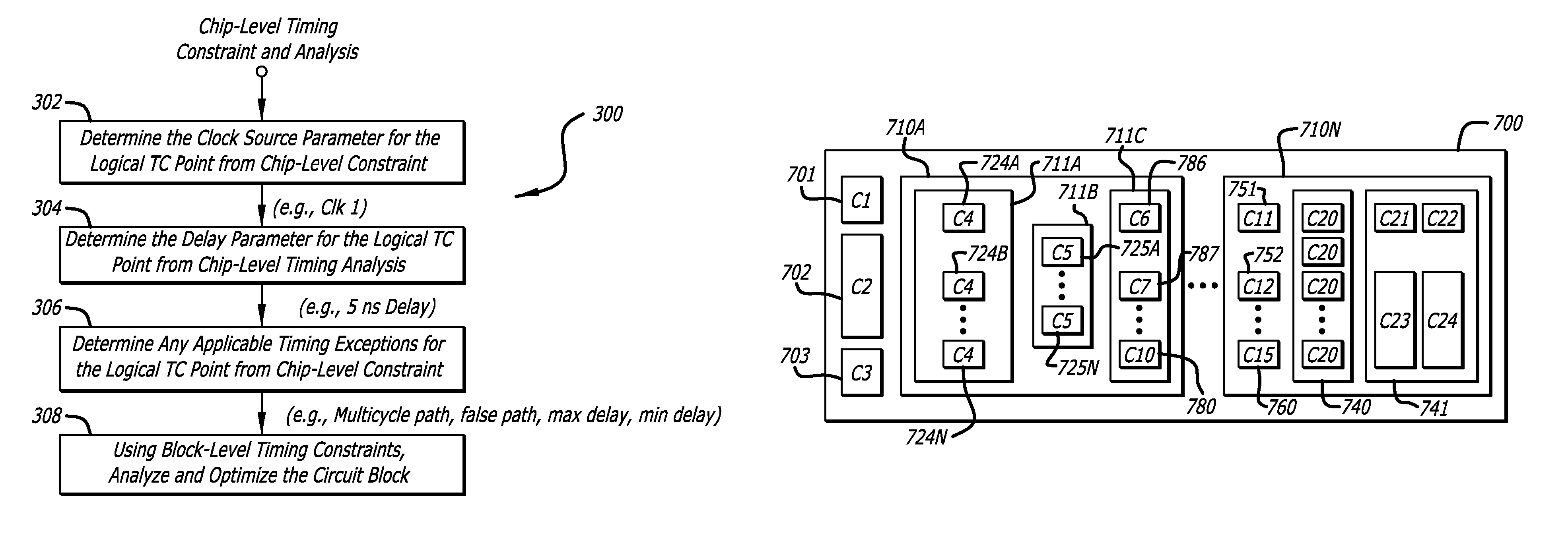
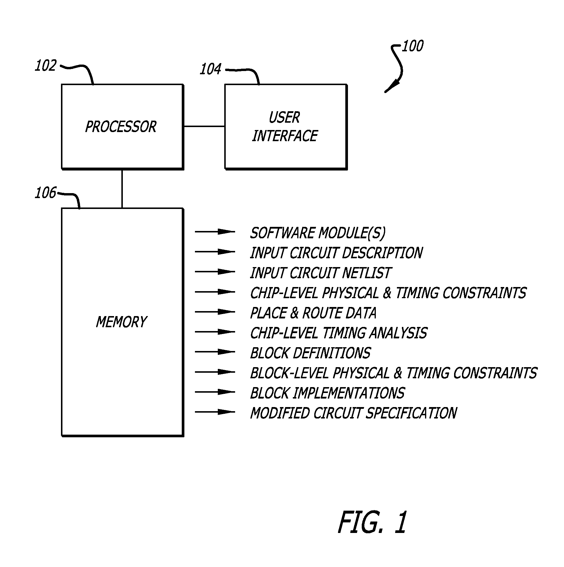
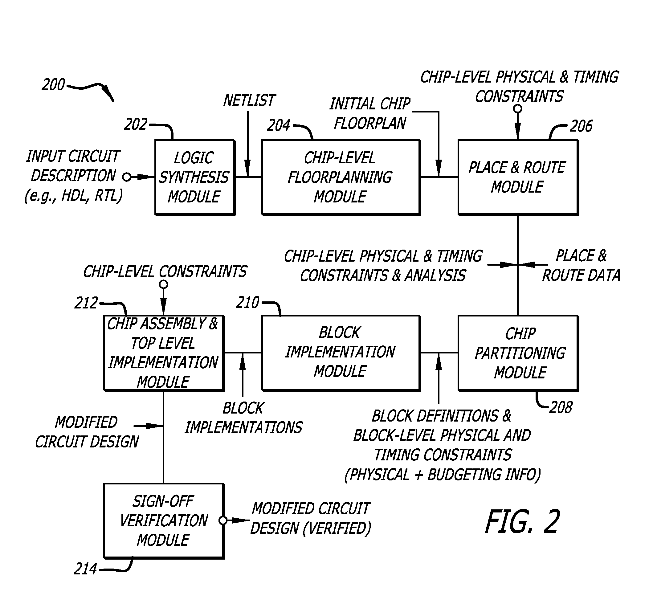
[0015]FIG. 1 illustrates a block diagram of an exemplary circuit design system 100 for designing integrated circuits in accordance with an embodiment of the invention. As discussed in more detail below, the circuit design system 100 is capable of generating timing constraints for individual hierarchical blocks of an integrated circuit that are derived from the chip-level timing constraints and analysis. Using the chip-level timing constraints and analysis, the circuit de...


PUM


Abstract

A system and method of designing an integrated circuit capable of deriving timing constraints for individual block-level circuits of an integrated circuit that are derived from the chip-level timing constraints and analysis. The block-level timing constraints are in the form of one or more logical timing constraint points at the input and output ports of block-level circuits. Each logical timing constraint points specifies a clock source used to clock data through the port, a delay parameter specifying data propagation delay backward from an input port and forward from an output port, and any timing exception associated with the data path. Using the logical timing constraint point, the circuit design system performs independent timing analysis and optimization of each block-level circuit. The system then reassembles the block-level circuits into a modified chip-level circuit for which timing closure can be achieved.

Description

FIELD OF THE INVENTION[0001]This invention relates generally to integrated circuit design systems, and in particular, to a system and method of generating hierarchical block-level timing constraints from chip-level timing constraints.BACKGROUND OF THE INVENTION[0002]Integrated circuits have become extremely large and complex, typically including millions of components. It follows then that the design of integrated circuits is also very complex and time consuming, involving synthesizing, analyzing and optimizing many circuit parameters. Because of this complexity, electronic design automation (EDA) systems have been developed to assist designers in developing integrated circuits at multitude levels of abstraction.[0003]In many cases, an integrated circuit under development may be so complex that even EDA systems have difficulties in achieving design closure within a reasonable time period. Thus, there is a need for a system and method to reduce the time required to achieve design clo...

Claims


Application Information

Patent Timeline
Patent Type & Authority Patents(United States)
IPC IPC(8): G06F17/50
CPCG06F17/5031G06F17/505G06F2217/84G06F30/3312G06F30/327G06F2119/12
Inventor LEVITSKY, OLEGKUO, CHIEN-CHUGUPTA, DINESH
Owner CADENCE DESIGN SYST INC
Why Eureka
Try Eureka