
Semiconductor light-emitting device

a technology semiconductors, which is applied in the direction of solid-state devices, instruments, material analysis, etc., can solve the problems of restricted light output efficiency of such conventional structures, difficulty in mounting led elements of reduced size, and conventional structures and methods, so as to reduce the number of production steps, simplify the structure of semiconductor light-emitting devices, and reduce the number of parts.

Inactive Publication Date: 2011-04-26
ACCELERATE DEVICE
View PDF5 Cites 20 Cited by
  • Summary
  • Abstract
  • Description
  • Claims
  • Application Information

AI Technical Summary

Benefits of technology

"The invention provides a semiconductor light-emitting device that combines the benefits of both top-view and side-view structures in one monolithic structure. This results in improved light output efficiency even in small chip sizes and relatively reduced structures compared to conventional devices. The device includes a light-emitting semiconductor element, a transparent resin mold covering the semiconductor element and the lead frame, and a reflective surface formed on a bent portion of the lead frame. The structure of the device is simplified and minimized as the number of parts and production steps can be reduced. The device can correspond to either of top- and side-view type configurations. Overall, the invention provides a novel and improved semiconductor light-emitting device with improved light output efficiency and a more minimized structure."

Problems solved by technology

Conventional structures and methods discussed above can have a difficulty in mounting an LED element of reduced size.
Also, the light output efficiency of such conventional structures can be restricted.

Method used


Image

  • Semiconductor light-emitting device
  • Semiconductor light-emitting device
  • Semiconductor light-emitting device

Examples


Embodiment Construction

[0027]Hereinafter, examples of devices embodying the invention will be described in detail in order to illustrate different embodiments of the invention and certain examples of devices, systems and methods that include such embodiments and that are possible given the novel and useful inventive concepts and discoveries described herein. In the description below, several embodiments are set out with different examples of configurations, alternative components or operational blocks, and related operations. Though various examples describe alternative embodiments, where different components or operational blocks are intended as optional. The invention is directed to broad concepts described below, and are not limited to any particular embodiment or configuration, but extends to the scope defined by the appended claims and all equivalents.

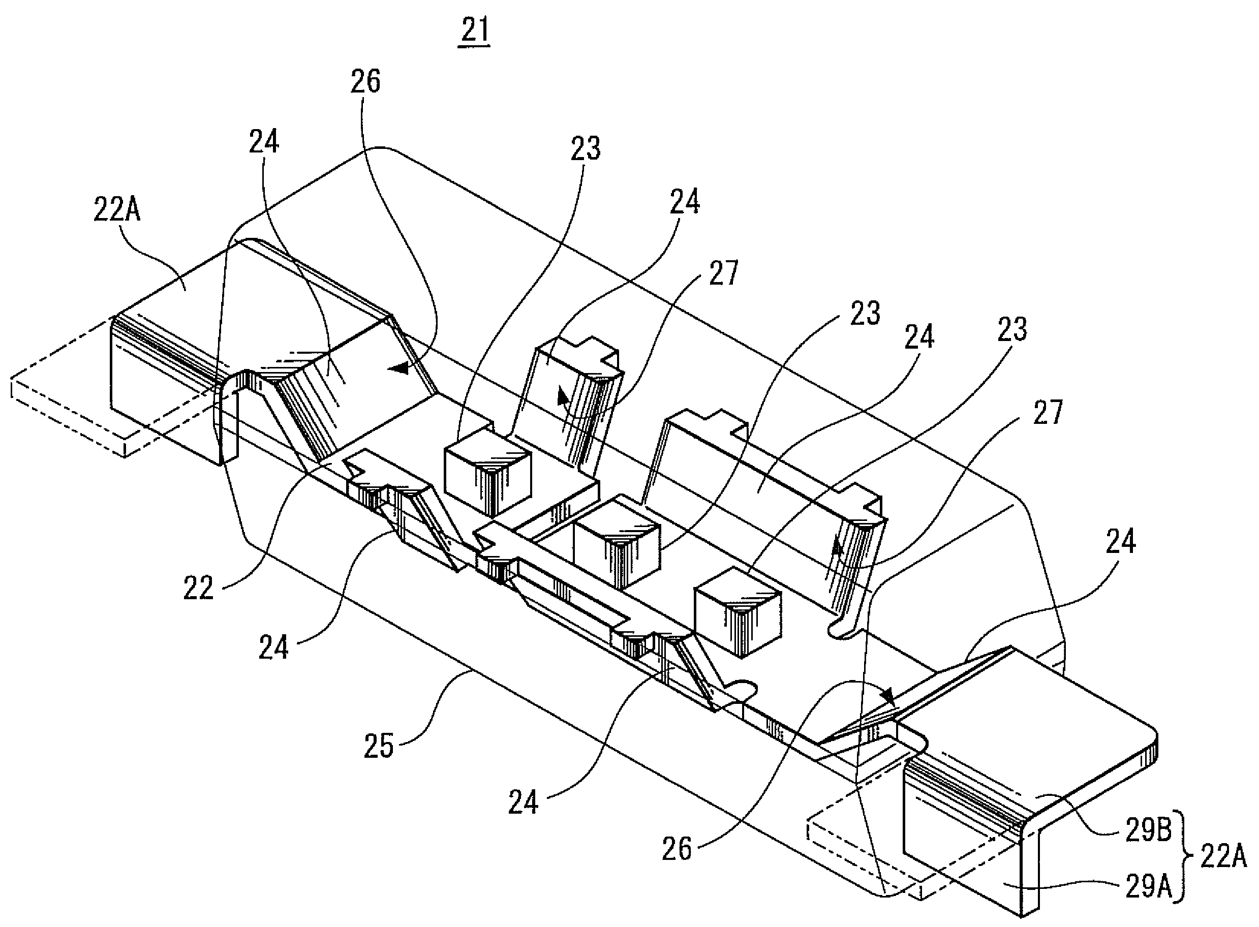
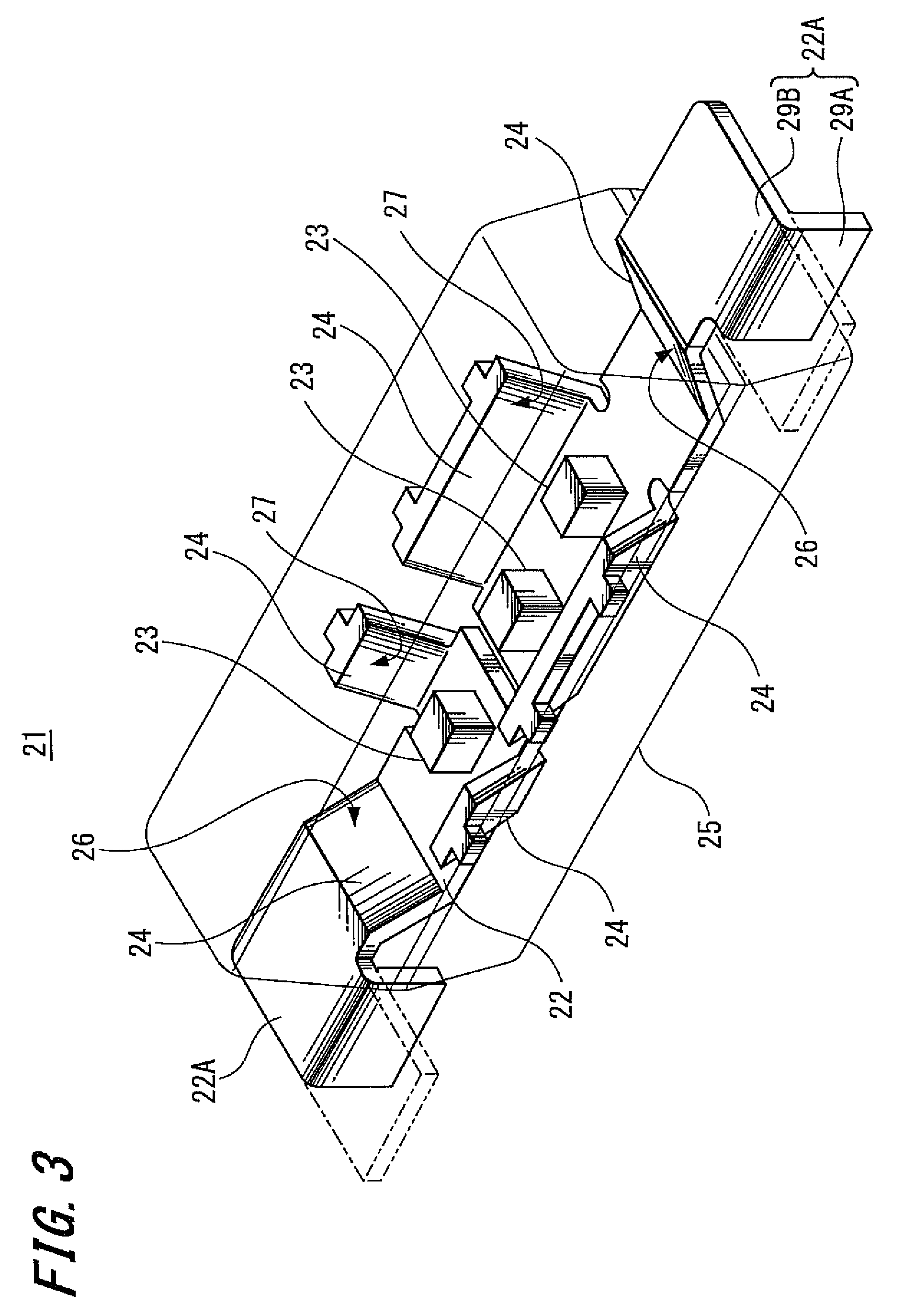
[0028]FIG. 3 shows a semiconductor light-emitting device configured according to an embodiment of the invention. A semiconductor light-emitting device ...


PUM


Abstract

A semiconductor light-emitting device includes: a light-emitting semiconductor element arranged on a lead frame; a transparent resin mold covering the light-emitting semiconductor element and the lead frame except a terminal portion of the lead frame; and a reflective surface formed on a bent portion of part of the lead frame. The terminal portion of the lead frame has a terminal structure, which can serve as a combination of a top-view type and a side-view type.

Description

CROSS REFERENCES TO RELATED APPLICATIONSRelated Application Data[0001]This application and all related applications claim the benefit of parent Japanese Patent Application JP 2007-141420 filed in the Japanese Patent Office on May 29, 2007, the entire contents of which are hereby incorporated herein by reference. This application thus has the priority filing date of May 29, 2007.BACKGROUND OF THE INVENTION[0002]The invention relates to a semiconductor light-emitting device, which can be applied to a backlight of a liquid crystal display element, a flash light source of a portable camera, or the like.DESCRIPTION OF THE RELATED ART[0003]Semiconductor light-emitting devices using light-emitting diode elements, which can be applied to a backlight of liquid crystal display elements in portable devices, a flash light source of cameras in portable devices, or the like, have been developed. For illustration in contrast to the invention, examples of conventional semiconductor light-emitting d...

Claims


Application Information

Patent Timeline
Patent Type & Authority Patents(United States)
IPC IPC(8): H01L29/20H01L33/00H01L31/14H01L33/50H01L33/54H01L33/56H01L33/60H01L33/62
CPCH01L33/486H01L33/62H01L33/60H01L25/0753H01L25/167H01L2224/48091H01L2224/48137H01L2924/01078H01L2924/01079H01L2224/48465H01L2224/48247H01L2224/45144H01L2924/00014H01L2924/00H01L2224/8592
Inventor OSAMU, ABE
Owner ACCELERATE DEVICE
Learn More