Method for annealing photovoltaic cells

a photovoltaic cell and annealing technology, applied in photovoltaic energy generation, electrical equipment, coatings, etc., can solve the problems of difficult industrial application and uneconomical viable methods

Active Publication Date: 2011-05-03
COMMISSARIAT A LENERGIE ATOMIQUE ET AUX ENERGIES ALTERNATIVES
View PDF5 Cites 2 Cited by
  • Summary
  • Abstract
  • Description
  • Claims
  • Application Information

AI Technical Summary

Benefits of technology

[0015]Thus, according to an embodiment of the invention, the photovoltaic cell undergoes at least two successive annealing steps. The first annealing operation, similarly to the methods of the prior art, enables the migration of hydrogen in ion form from the antireflection layer into the substrate if said antireflection layer is hydrogen-rich. The hydrogen diffused in the substrate can also be obtained by a step of hydrogenation of the substrate. The second annealing operation, which is performed at a much lower temperature than the first annealing operation, enables the diffused hydrogen to form additional bonds with crystallographic defects or impurities present in the substrate. Thus, the lifetime of the carriers in the substrate is prolonged, thus enhancing the efficiency of the photovoltaic conversion of the cell. In addition, this second annealing operation does not require any pressure or gas constraints, unlike the annealing operations under H2 and N2 of the prior art, which represents a significant economic advantage.

Problems solved by technology

The cell obtained offers an efficiency slightly above 18% with a P-type multicrystalline silicon substrate obtained by tape drawing, but the method proposed is not economically viable and is difficult to apply industrially.

Method used


Image

  • Method for annealing photovoltaic cells
  • Method for annealing photovoltaic cells
  • Method for annealing photovoltaic cells

Examples


Embodiment Construction

[0009]Thus there is a need to propose a method for annealing photovoltaic cells making it possible to obtain photovoltaic cells that are more efficient than the cells produced according to the methods of the prior art described above, and that are economically viable in the industry.

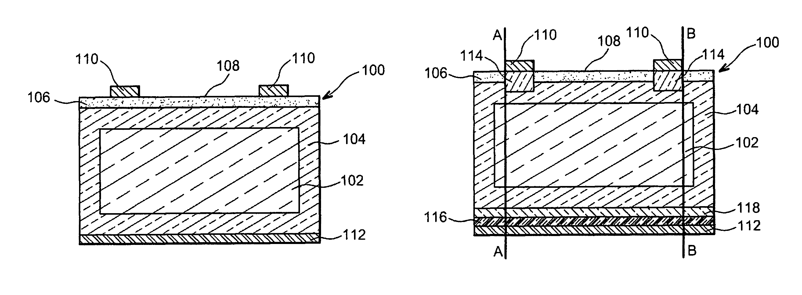
[0010]An embodiment of the present invention proposes a method for annealing at least one photovoltaic cell comprising a substrate based on a semiconductor, for example silicon, with a first type of conductivity, a layer doped with a second type of conductivity produced in the substrate and forming a front face of the substrate, an antireflection layer produced on the front face of the substrate and forming a front face of the photovoltaic cell, at least one metallization on the front face of the photovoltaic cell and at least on metallization on a rear face of the substrate, which method comprising at least the steps of:

[0011]a) a first annealing of the photovoltaic cell at a temperature between around ...


PUM


Abstract

Method for annealing at least one photovoltaic cell comprising a substrate based on silicon with a first type of conductivity, a layer doped with a second type of conductivity produced in the substrate and forming a front face of the substrate, an antireflection layer produced on the front face of the substrate and forming a front face of the photovoltaic cell, at least one metallization on the front face of the cell and at least on metallization on a rear face of the substrate. This method comprises at least the steps of:a) a first annealing of the photovoltaic cell at a temperature between around 700° C. and 900° C.,b) a second annealing of the photovoltaic cell at a temperature between around 200° C. and 500° C., at ambient pressure and in ambient air,with hydrogen being diffused in the substrate during the process.

Description

TECHNICAL FIELD AND PRIOR ART[0001]This invention relates to the field of photovoltaic cells and more specifically a method for annealing photovoltaic cells.[0002]A standard method used for the industrial production of a photovoltaic cell 20 based on P- or N-type crystalline (monocrystalline or multicrystalline) silicon is shown in FIGS. 1A to 1E. An N- or a P-type substrate 2 first undergoes a texturisation of its surfaces by use of a potassium hydroxide solution, making it possible to reduce the reflectivity of these surfaces and thus obtain a better optical confinement of the beams entering the substrate 2. An N+ type layer 4 is formed in the substrate 2 by diffusion of phosphorus at the level of all of the faces of the substrate 2 (FIG. 1A). An antireflection layer 6 of hydrogen-rich silicon nitride (SiN—H) is then deposited on the N+ layer 4 by plasma-enhanced chemical vapour deposition (PECVD), as shown in FIG. 1B, forming a front face 8 of the photovoltaic cell 20. Silver 10 ...

Claims


Application Information

Patent Timeline
Patent Type & Authority Patents(United States)
IPC IPC(8): H01L21/00H01L31/00
CPCH01L31/1864H01L31/1868Y02E10/547Y02P70/50
Inventor ENJALBERT, NICOLASDUBOIS, SEBASTEIN
Owner COMMISSARIAT A LENERGIE ATOMIQUE ET AUX ENERGIES ALTERNATIVES
Why Eureka
Try Eureka