Heater chips with silicon die bonded on silicon substrate and methods of fabricating the heater chips

a technology of heater chips and silicon substrates, applied in metal-working devices, printing, writing implements, etc., can solve the problems of long-term corrosion problems, limited printing quality, and less than simple manufacturing, and achieve the effect of low cost and precis

Inactive Publication Date: 2011-05-10
FUNAI ELECTRIC CO LTD
View PDF4 Cites 9 Cited by
  • Summary
  • Abstract
  • Description
  • Claims
  • Application Information

AI Technical Summary

Benefits of technology

[0012]The present invention meets this need by providing an innovation which allows replacement of the traditional adhesive die bonding of the chip module to the base plate of the plastic ink bottle which required curing at a high temperature causing expansion and contraction cycling during cooling which is a major contributor to poor heater chip and nozzle plate alignment as well as warping and bowing due to mismatch of CTE between components which compromises nozzle plate planarity, resulting in misdirection of ink drop jetting from the nozzle holes. Underlying the innovation of the present invention is the insight that by devising a different construction for the heater chip through a different method for fabricating the heater chip, in which, by separately processing a carrier wafer of silicon for making silicon substrates, to serve the function of base plates, and a device wafer of silicon for making silicon dies, and non-adhesively bonding the carrier and device wafers to one another, and dicing the bonded wafers into the chip modules, the need to utilize an adhesive die bond attachment of the heater chip of the chip module to the plastic base plate of the ink bottle could be eliminated and a suitable non-adhesive mechanical attachment of the heater chip to the ink bottle could be substituted in its place, eliminating the deleterious effects on the heater chip of the adhesive attachment process in terms of warping and bowing which adversely impact print quality. Alternatively, by dicing the device wafer into dies before the bonding thereof to the carrier wafer, bonding the diced dies to the substrates of the carrier wafer and dicing the carrier wafer into substrates laden with plural dies, chip modules are produced having multiple dies.
[0013]Other advantages which will become apparent hereinafter relating to cost reduction of printhead chip module fabrication and tailoring of printhead chip module construction for the particular application can also be gained by the insight underlying the present invention of separate processing of carrier and device wafers for respectively making arrays of substrates and dies for bonding together and dicing into chip modules. This allows the relative makeup and size of the substrate and die(s) to be separately tailored for the particular conditions of a given application for meeting the goal of precise construction and operation at low cost while still maintaining or improving print quality.
[0019]Thus, the heater chip and its fabrication methods of the present invention provide a solution to the aforementioned problems associated with the prior art printhead chip module design in that the necessity of an adhesive die bond attachment of the heater chip of the chip module to the ink bottle is obviated by processing the carrier wafer for substrates and the device wafer for dies separately and then forming a bond between them that is non-adhesive and hermetic in nature and cures at room temperature, which avoids the cycling of expansions and contractions during cooling as occurs in the case of the prior art adhesive die bonding of the prior art heater chip to the ink bottle which is a major contributor to poor chip planarity and reduced print quality. Thus, due to the separate processing of the carrier wafer of an increased size to resist bowing, the necessity to utilize an adhesive die bond attachment of the heater chip of the chip module to a plastic base plate of an ink bottle, if desired, to complete assembly of the printhead chip module is avoided and substitutable in its place is a non-adhesive attachment of the heater chip to the ink bottle.
[0020]Various alternative embodiments, enhancements and other aspects of the heater chip and its fabrication method of the present invention that are disclosed hereinafter allow the balancing of tradeoffs between chip size, performance requirements, industry cost reduction trends and other factors so as to allow tailoring of heater chip and silicon substrate parameters to achieve a low-cost and precise construction that provides a given ink flow rate into the smaller spaces of one or more miniaturized heater chips.

Problems solved by technology

The conventional design, illustrated in FIGS. 1 and 2 and similarly disclosed in U.S. Pat. No. 6,402,301, which is hereby incorporated by reference in its entirety, is effective for today's print quality demands; however, it is apparent that the system described above has print quality limitations, invites long-term corrosion issues, and is less than simple to manufacture.
Regarding ink drop misdirection, anomalies which cause it are ones that adversely affect nozzle planarity, bore angle of nozzle sidewalls, ink drop velocity, heater / nozzle plate alignment, and dimensional relationships between components.
If the nozzle plate is warped or bowed, the desired direction of the ink-jetting is compromised.
Further affecting nozzle planarity are planarity of the base plate in the bottle, non-uniform deposition of either the FF material or a photo-imageable nozzle plate layer impacting formation of the nozzle holes, and sagging of the nozzle plate into the via due to lack of support over the via causing misdirection of nozzle holes.
Current technologies are severely limited in their ability to repeatably produce this feature.
Ink drop velocity is adversely affected by distortion of the dimensions of the heater elements and the size of the ink ejection chambers.
Heater size is limited by the heater chip surface space.
The heater chip / nozzle plate alignment in the chip module is affected by how well the nozzle plate is aligned with the heater elements, which is proving to be very difficult to accomplish.
Also, expansion and contraction of the nozzle plate resulting from other wet and dry processing will affect this alignment.

Method used


Image

  • Heater chips with silicon die bonded on silicon substrate and methods of fabricating the heater chips
  • Heater chips with silicon die bonded on silicon substrate and methods of fabricating the heater chips
  • Heater chips with silicon die bonded on silicon substrate and methods of fabricating the heater chips

Examples


Embodiment Construction

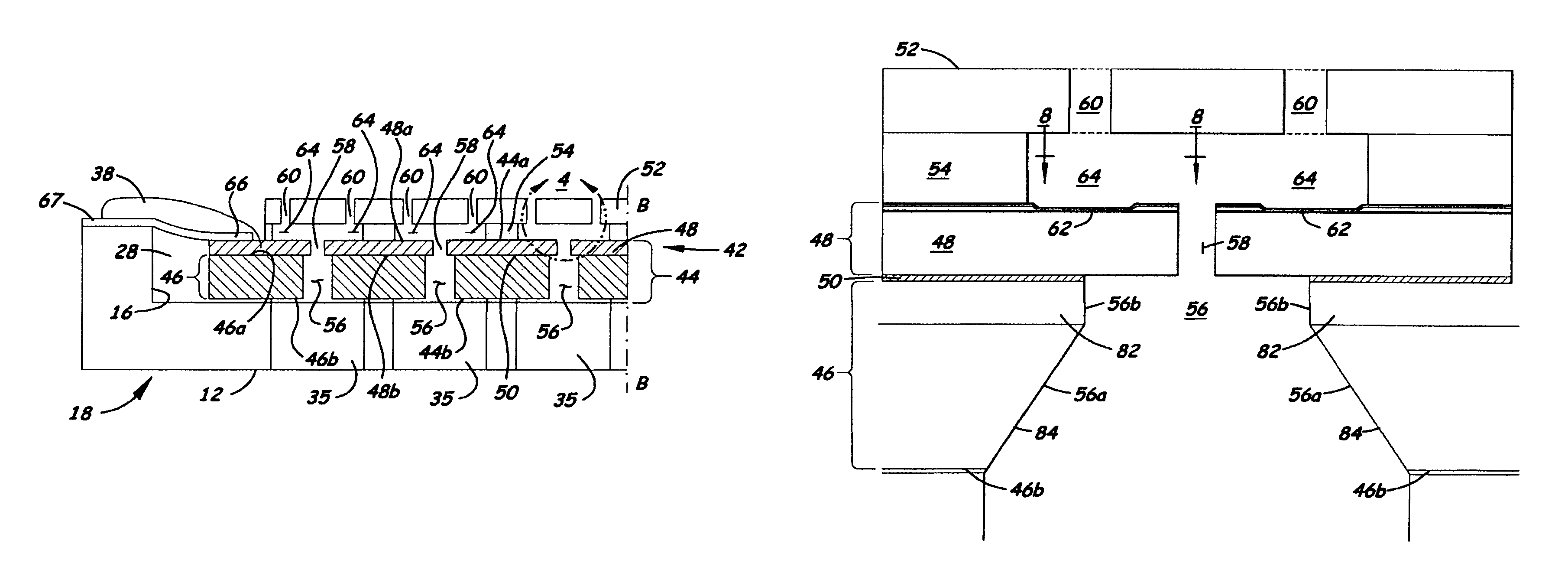
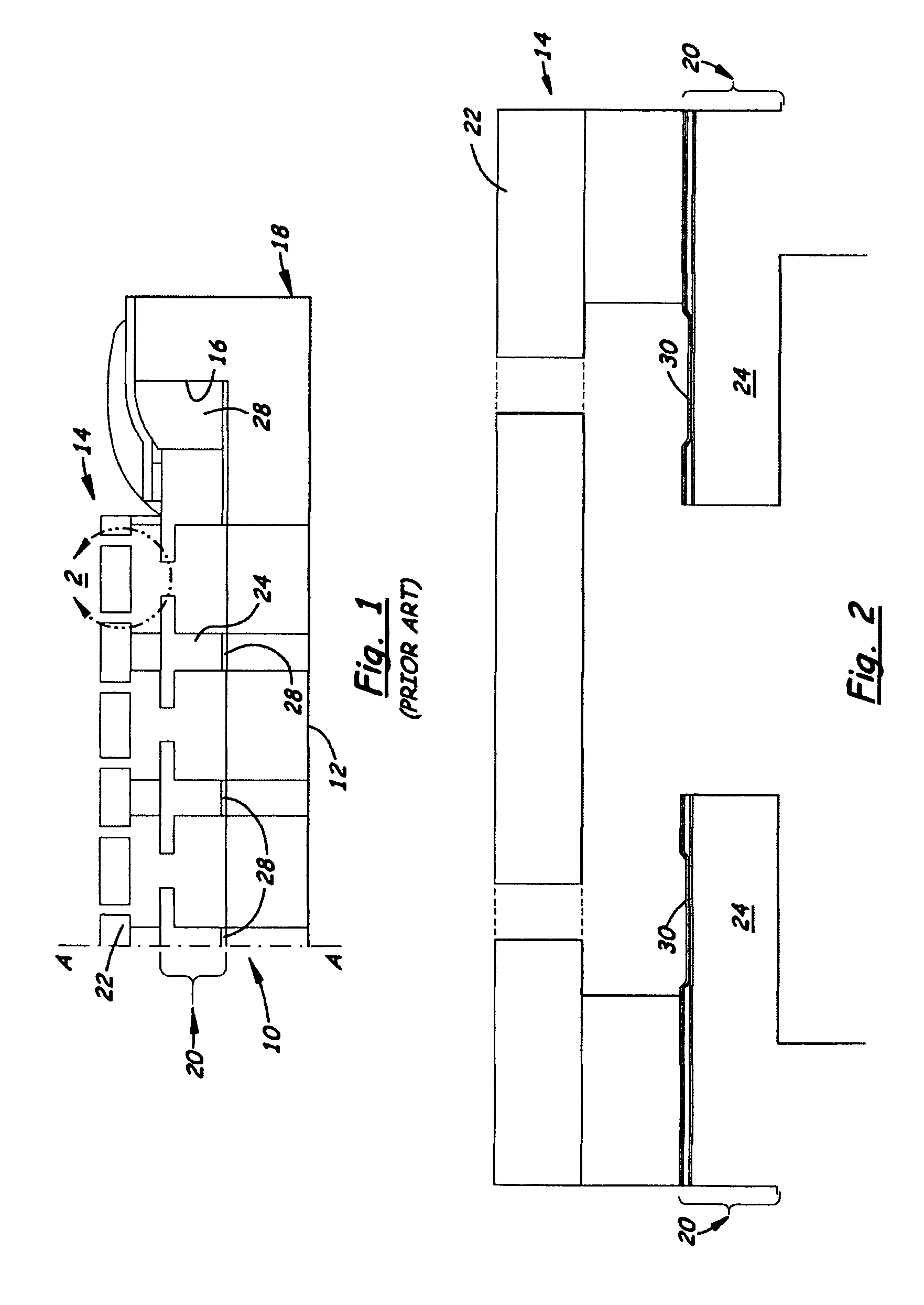
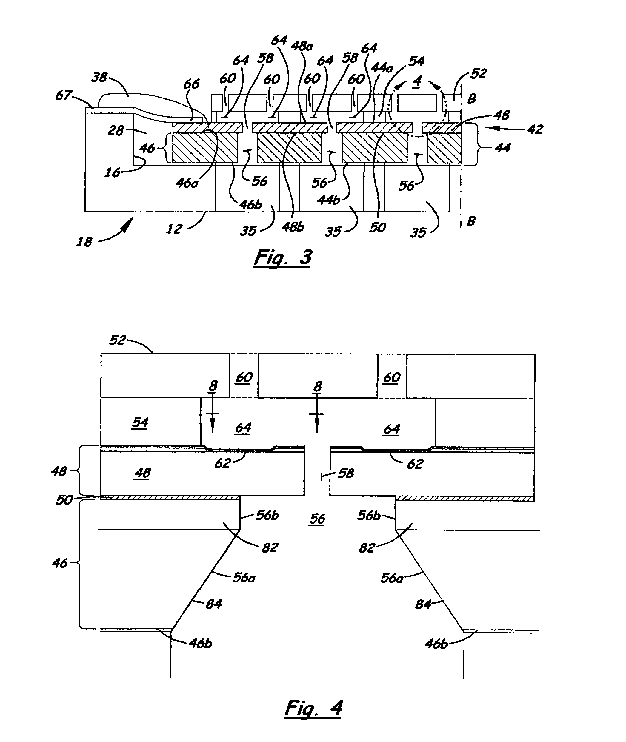
[0035]The present invention now will be described more fully hereinafter with reference to the accompanying drawings, in which some, but not all, embodiments of the invention are shown. Indeed, the invention may be embodied in many different forms and should not be construed as limited to the embodiments set forth herein; rather, these embodiments are provided so that this disclosure will satisfy applicable legal requirements. Like numerals refer to like, comparable or corresponding elements throughout the views.

[0036]Also, it should be understood that the invention applies to any micro-fluid ejection device, not just to thermal inkjet heater chips. While the embodiments of the invention will be described in terms of a thermal inkjet printhead, one of ordinary skill will recognize that the invention can be applied to any micro-fluid ejection system.

[0037]Further, it should be understood that many of the embodiments of the invention employ low temperature bonding technology which is ...


PUM

PropertyMeasurementUnit
thickaaaaaaaaaa
thicknessaaaaaaaaaa
thicknessaaaaaaaaaa

Abstract

A heater chip has a substrate and at least one die, made of silicon, and a bond non-adhesively attaching them. The substrate, thick enough to resist bowing, has ink supply vias from back to front surfaces. The die has ink flow vias from back to front surfaces and circuitry including heater elements adjacent the front surface interspersed with ink flow vias. The at least one die is superimposed on the substrate such that ink supply vias of the substrate align with ink flow vias of the die and portions of substrate front surface and die back surface are aligned, disposed adjacent and facing one another. The bond formed between substrate and die facing surface portions is hermetic and equal in strength to a Si—O bond. By separate processing of carrier and device wafers, size and features of substrate and die can be tailored to provide a desired heater chip construction.

Description

CROSS REFERENCE TO RELATED APPLICATION[0001]This patent application is related to the U.S. patent application Ser. No. 11 / 848,246, filed Aug. 31, 2007, entitled “Micro-Fluid Ejection Heads And Methods For Bonding Substrates To Supports” and assigned to the assignee of the present application.BACKGROUND[0002]1. Field of the Invention[0003]The present invention relates generally to fluid ejection modules and, more particularly, to a heater chip for an inkjet printhead chip module having a silicon die bonded on a silicon substrate and methods of fabricating the heater chip.[0004]2. Description of the Related Art[0005]A thermal inkjet printhead is used in a variety of products, such as printers, copiers, faxes and the like, to form and propel drops of ink onto a sheet of print medium, such as paper. In general, an image is produced by the ink drops being emitted from the printhead at precise moments such that they impact the print medium at a desired location. The printhead is supported...

Claims


Application Information

Patent Timeline
Patent Type & Authority Patents(United States)
IPC IPC(8): B41J2/05B21D53/76
CPCB41J2/1603B41J2/1629B41J2/1631B41J2/164H01L21/6715B41J2/1632Y10T29/49401
Inventor ANDERSON, FRANK EDWARDBERNARD, DAVID LAURIERDRYER, PAUL WILLIAMJOYNER, II, BURTON LEEMCNEES, ANDREW LEESTRUNK, TIMOTHY LOWELLSULLIVAN, CARL EDMOND
Owner FUNAI ELECTRIC CO LTD
Why Eureka
Try Eureka