Atomic layer epitaxy processed insulation

a technology of atomic layer epitaxy and processed insulation, which is applied in the direction of polycrystalline material growth, crystal growth process, chemically reactive gas, etc., to achieve the effect of poor surface selectivity and facilitate the addition of surface coatings

Inactive Publication Date: 2011-05-24
SIEMENS ENERGY INC
View PDF16 Cites 3 Cited by
  • Summary
  • Abstract
  • Description
  • Claims
  • Application Information

AI Technical Summary

Benefits of technology

[0007]Each film layer deposited by the ALE may be a part of a composite layer of film depositions. Since the ALE deposits extremely small amounts of material, forming films about 1-10 molecules thick, it may be desirable to apply 2 or more depositions to create a sufficiently thick composite layer. In addition, however, each of the sub-layers in a composite film may have different materials deposited. This may be done to provide different or complimentary benefits.

Problems solved by technology

Due to poor surface selectivity and the mixed molecular nature of insulative tapes, particularly mica tapes, the materials deposited by ALE will readily bind to these surfaces.

Method used


Image

  • Atomic layer epitaxy processed insulation
  • Atomic layer epitaxy processed insulation
  • Atomic layer epitaxy processed insulation

Examples


Embodiment Construction

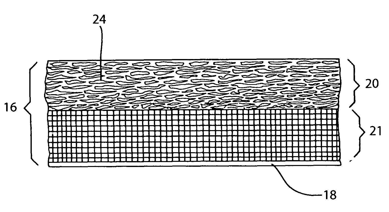
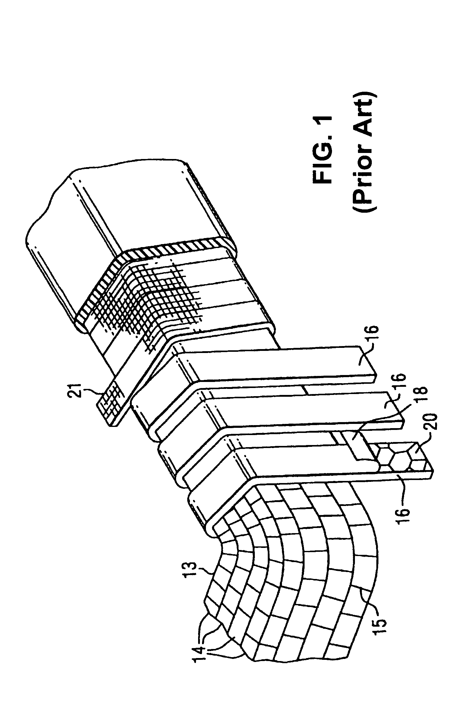
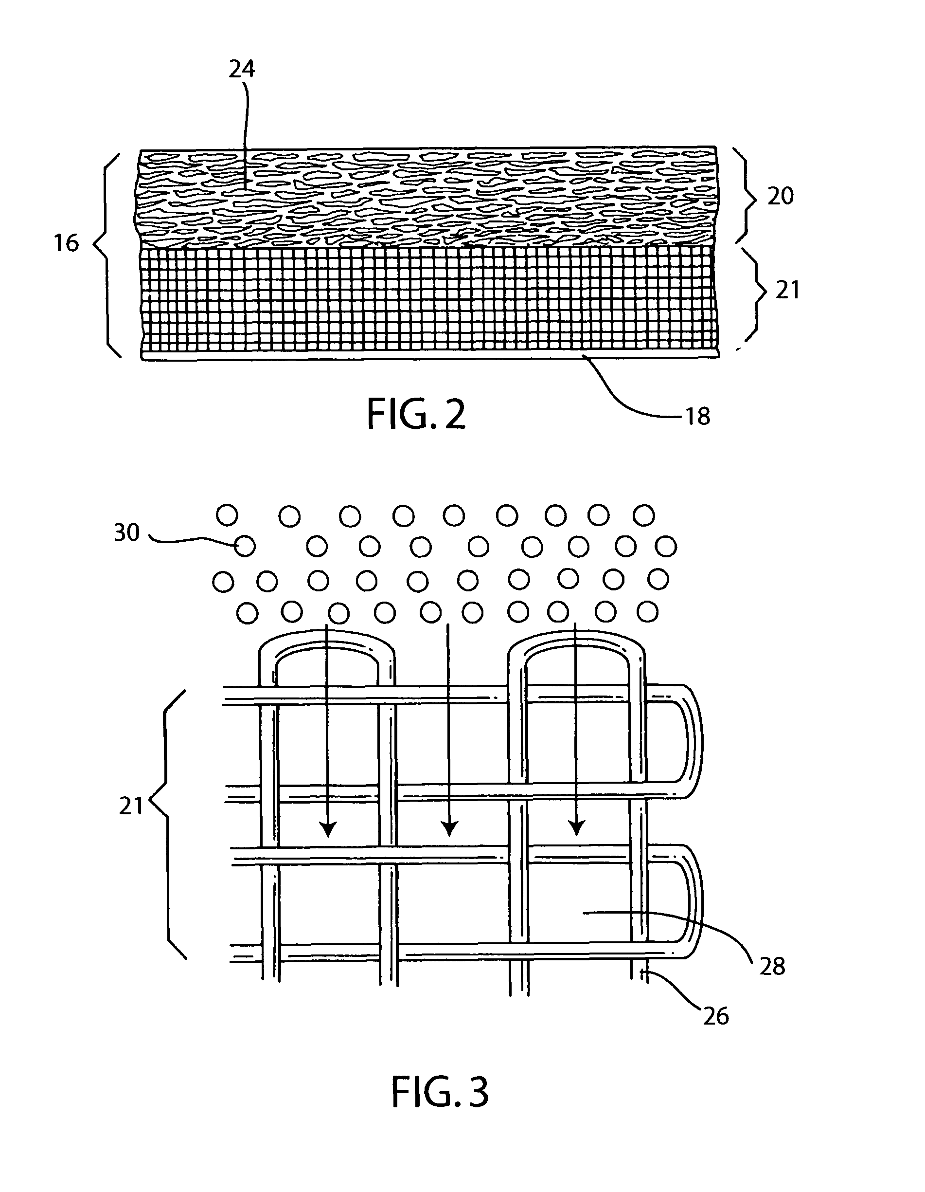
[0018]The present invention provides for a method and apparatus for depositing physically enhancing (PE) materials onto a composite tape via atomic layer epitaxy (ALE). Insulation such as composite tapes are very important in electrical systems to prevent voltage breakdown. Unfortunately, while guarding against voltage breakdown, the composite tapes also impede other desirable characteristics such as thermal conductivity, mechanical strength and general durability.

[0019]These other physical properties of the tapes can be enhanced by the addition of PE materials added directly to the various tape components. The PE materials are metallic and non-metallic inorganic oxides, nitrides, carbides or organometalics that form thin film layers on surfaces of the composite tape. The thin film layers may be applied to the surface of the tape as a whole and / or component layers, such as the fiber backing or individual mica flakes, which can then be combined to form the whole tape.

[0020]Atomic Lay...


PUM

PropertyMeasurementUnit
thermally conductiveaaaaaaaaaa
thickaaaaaaaaaa
electrically insulateaaaaaaaaaa

Abstract

In one embodiment the present invention provides for a method for depositing a thin film layer onto a composite tape 16, that comprises depositing at least one thin film layer of physically enhancing material 30 onto at least one portion of the composite tape. The depositing is accomplished by atomic layer epitaxy and the thin film layer is approximately 1-10 molecules thick.

Description

FIELD OF THE INVENTION[0001]The field of the invention relates to the deposit of materials and layers to insulation via atomic layer epitaxy.BACKGROUND[0002]With the use of any form of electrical appliance, there is a need to electrically insulate conductors. With the push to continuously reduce the size and to streamline electrical and electronic systems there is a corresponding need to find better and more compact insulators and insulation systems.[0003]Good electrical insulators, by their very nature, also tend to be good thermal insulators, which is undesirable. Thermal insulating behavior, particularly for air-cooled electrical equipment and components, reduces the efficiency and durability of the components as well as the equipment as a whole. It is desirable to produce electrical insulation systems having maximum electrical insulation and minimal thermal insulation characteristics.[0004]Electrical insulation often appears in the form of insulating tapes, which themselves have...

Claims


Application Information

Patent Timeline
Patent Type & Authority Patents(United States)
IPC IPC(8): C30B21/04
CPCC23C16/45525
Inventor CONLEY, DOUGLAS J.
Owner SIEMENS ENERGY INC
Why Eureka
Try Eureka