Semiconductor package and method of making the same

a technology of semiconductor and packaging, applied in the direction of semiconductor/solid-state device details, semiconductor devices, electrical equipment, etc., can solve the problems of increased packaging cost and process steps, increased equipment investment, and additional process steps, so as to reduce or eliminate dependence

Active Publication Date: 2011-05-24
UTAC HEADQUARTERS PTE LTD
View PDF12 Cites 44 Cited by
  • Summary
  • Abstract
  • Description
  • Claims
  • Application Information

AI Technical Summary

Benefits of technology

[0012]Unlike the known processes as described above, the wafers need not be fully processed in order to proceed with the die stacking process. That is, the wafer need not undergo both the through silicon interconnect formation and the wafer thinning processes before other chips can be stacked onto it. Instead, stacking of the chips may be accomplished on semi-processed wafers which would have completed the through silicon interconnect fabrication process but not the wafer thinning process. The un-thinned wafer provides support for the assembly as the chips are stacked onto it and as the stacked structure is molded.
[0013]After molding, the thinning of the wafer occurs. The mold material provides support to the assembly during thinning and continues to support the assembly for subsequent processes such as backside metallization / passivation, under bump metallization pad formation, wafer bumping, singulation, etc. The process of the present invention can, thus, reduce or eliminate reliance on the use of temporary bonded support carriers, which is important for thin wafer handling and equipment processing in the known process as described above.

Problems solved by technology

However, the process of bonding the support carrier to the wafer involves additional process and material developments, additional equipment investment, increased packaging cost and additional process steps directed to the bonding of the support carrier to and de-bonding of the support carrier from the wafer.
The known processes of forming the stacked die package involve the use of one or more support carriers which can result in the disadvantages as highlighted above.

Method used


Image

  • Semiconductor package and method of making the same
  • Semiconductor package and method of making the same
  • Semiconductor package and method of making the same

Examples


Embodiment Construction

[0037]The present invention will now be described more fully with reference to the accompanying drawings, in which exemplary embodiments of the invention are shown.

Stacked Package Having Two Dies

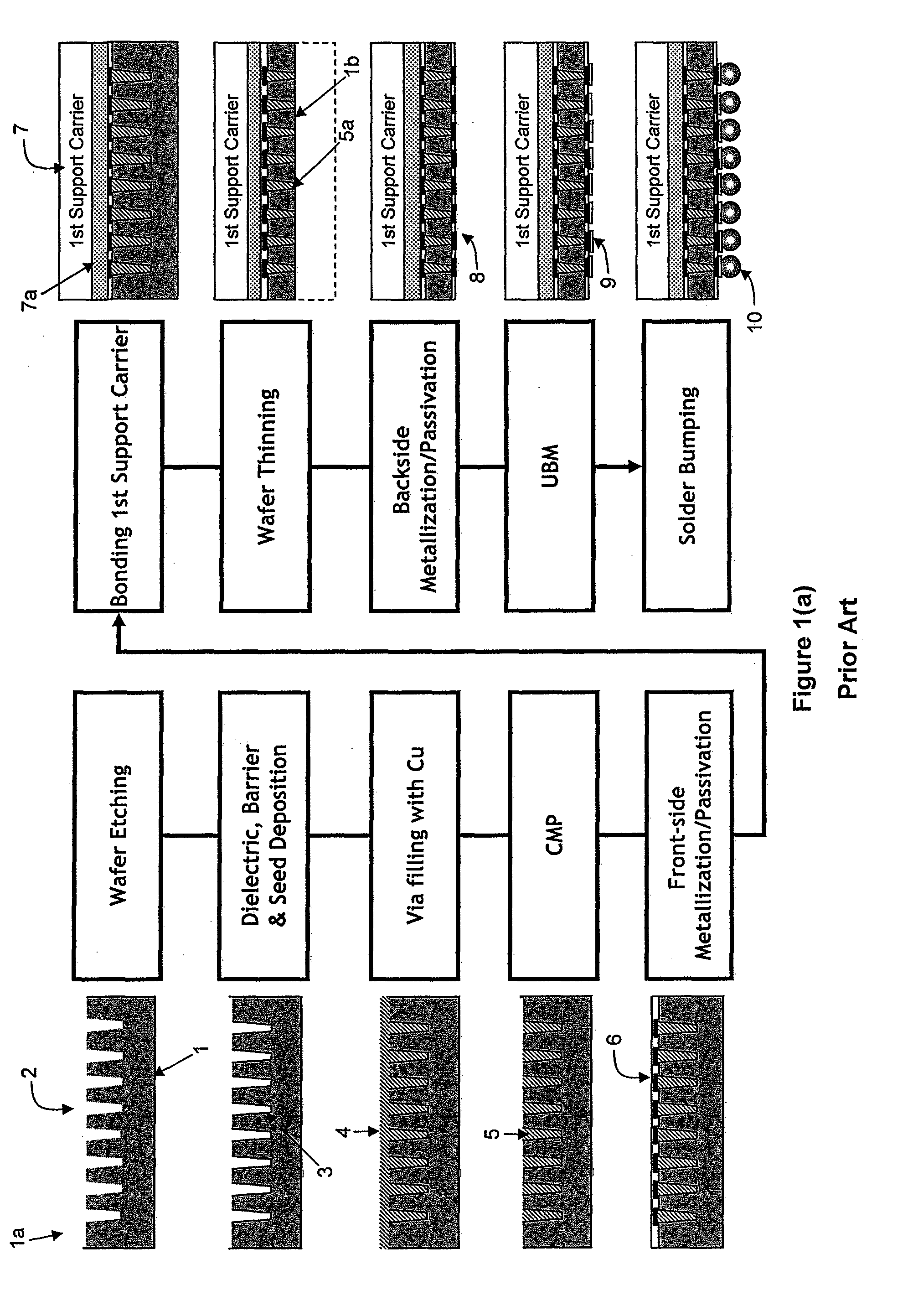
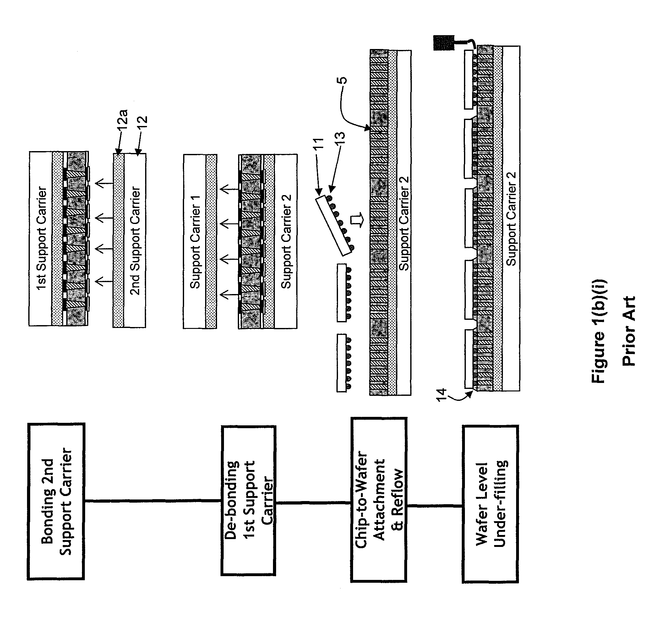
[0038]A process of making a semiconductor device is described with reference to the process flow diagram of FIGS. 2(a) to 2(o).

[0039]The process comprises the steps 1 to 15 which will be described in detail in the paragraphs below.

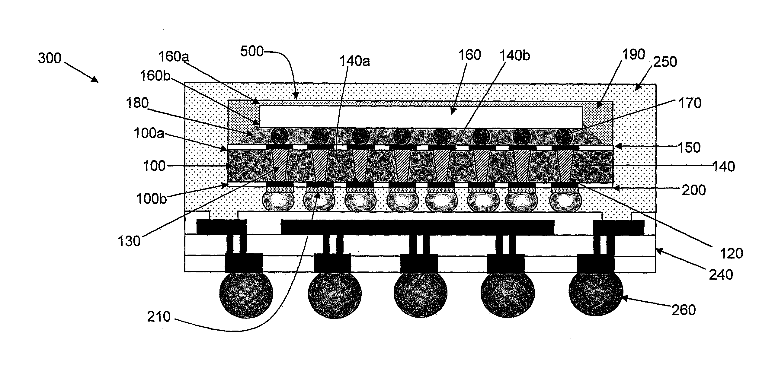
[0040]“Wafer Etching” step 1, FIG. 2(a):—A wafer 100 is etched to create one or more vias 110 in the wafer 100. The wafer can be an inactive silicon wafer without active circuitry embedded therein, or an active silicon wafer with active circuitry embedded therein. Where the wafer is an active wafer, it would result in a functional die in the resulting stacked die package. Where the wafer is an inactive wafer, it would function as an interposer for distributing finer pitch connections of the chip stacked above to larger pitch connections of the substrate below. The ...


PUM


Abstract

The present invention relates to semiconductor devices comprising two or more dies stacked vertically on top of one another, and methods of making the semiconductor devices. The methods may comprise a combination of wafer-level through silicon interconnect fabrication and wafer-level assembly processes.

Description

CROSS-REFERENCE TO RELATED PATENT APPLICATION[0001]The present application claims priority from U.S. Provisional Application No. 61 / 027,843, which was filed on Feb. 12, 2008, and is incorporated herein by reference in its entirety.BACKGROUND OF THE INVENTION[0002]1. Field of the Invention[0003]The present invention relates to semiconductor devices comprising two or more dies stacked vertically on top of one another, and methods of making the semiconductor devices.[0004]2. Description of the Related Art[0005]Vertical stacking of multiple flip chips in a stacked die package requires wafers to be processed with through silicon interconnects to enable face-to-back (F2B) flip chip bonding. The wafers are typically thinned or back-ground during the process of forming the interconnects, and therefore known processes for stacking the thinned wafers require a support carrier that is temporarily bonded to the wafers during handling and equipment processing to prevent warping. More particularl...

Claims


Application Information

Patent Timeline
Patent Type & Authority Patents(United States)
IPC IPC(8): H01L23/48H01L23/52
CPCH01L21/486H01L23/3128H01L23/3135H01L24/97H01L21/561H01L2924/01033H01L21/563H01L23/49827H01L2224/16225H01L2224/73204H01L2224/97H01L2924/01013H01L2924/01029H01L2924/01046H01L2924/01073H01L2924/01074H01L2924/01078H01L2924/01079H01L2924/04941H01L2924/15311H01L2924/01024H01L2924/01023H01L2924/01019H01L2924/01006H01L2924/01005H01L2224/81H01L24/03H01L24/05H01L2224/05001H01L2224/05009H01L2224/05023H01L2224/05568
Inventor NG, CATHERINE BEE LIANGTOH, CHIN HOCKSUN, ANTHONY YI-SHENG
Owner UTAC HEADQUARTERS PTE LTD
Why Eureka
Try Eureka