Plasma process etch-to-deposition ratio modulation via ground surface design

Inactive Publication Date: 2014-05-08
NOVELLUS SYSTEMS
View PDF3 Cites 4 Cited by
  • Summary
  • Abstract
  • Description
  • Claims
  • Application Information

AI Technical Summary

Benefits of technology

The present invention describes methods and apparatus for controlling the properties of a plasma in a plasma deposition environment. This is particularly useful in ionized physical vapor deposition (iPVD) gap fill applications. The invention achieves this by modifying the grounding path of the plasma, which has a significant impact on the energy of ions impacting the substrate and the etch-to-deposition ratio of the plasma flux. By adjusting the grounding surface's location, shape, and area, the plasma properties can be controlled without the need for complicated RF systems, resulting in improved performance and reduced likelihood of damage to underlying structures. Complete elimination of RF is also possible, providing more uniform ion energy distribution and reducing reactor complexity.

Problems solved by technology

Even in conjunction with the application of RF bias, self-sputtering induced by grounding path modulation narrows the impacting ion energy distribution, decreasing the likelihood of damage to underlying structures during deposition-etch processing.

Method used


Image

  • Plasma process etch-to-deposition ratio modulation via ground surface design
  • Plasma process etch-to-deposition ratio modulation via ground surface design
  • Plasma process etch-to-deposition ratio modulation via ground surface design

Examples


Embodiment Construction

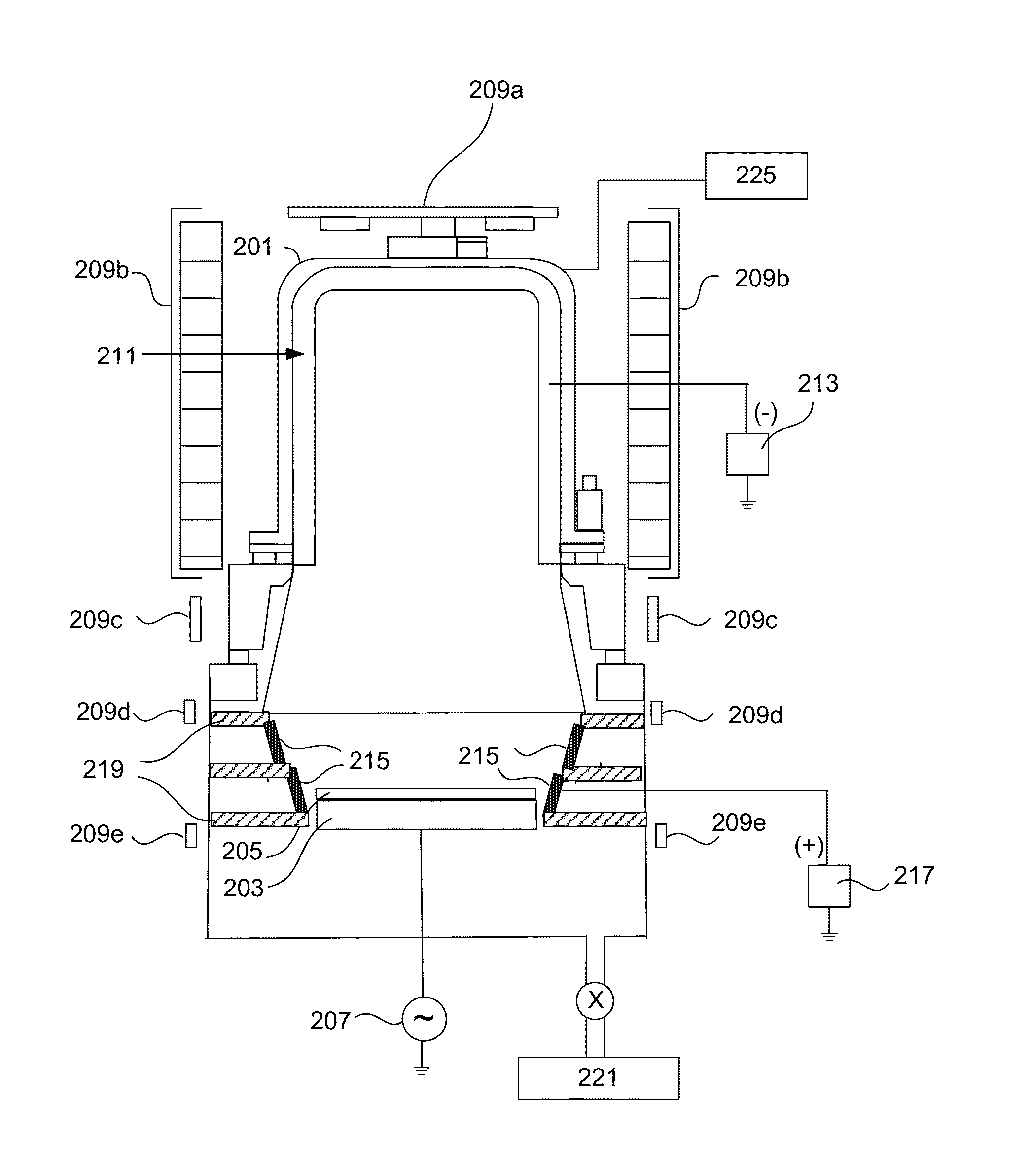
[0020]As noted above, the present invention relates to methods and apparatus for plasma deposition in which the properties of the plasma are controlled by modifying the grounding path of the plasma. The invention is potentially applicable in any plasma deposition environment, but finds particular use for filling recessed features on semiconductor substrates, for example by ionized physical vapor deposition (iPVD). According to various aspects of the invention, a discharge plasma is generated in a plasma reactor by ionization of a feed gas and sputtered material from a target. The discharge plasma includes metal and inert gas ions. The plasma circuit includes the target, the plasma itself, a grounding surface in the reactor, typically configured as a plurality of grounding shields, and a power supply that energizes the target. It has been found that the energy of ions impacting the substrate and etch-to-deposition ratio of the plasma flux can be controlled by modifying the grounding ...


PUM

PropertyMeasurementUnit
Electrical resistanceaaaaaaaaaa
Ratioaaaaaaaaaa
Surface areaaaaaaaaaaa

Abstract

Plasma deposition in which properties of a discharge plasma are controlled by modifying the grounding path of the plasma is potentially applicable in any plasma deposition environment, but finds particular use in ionized physical vapor deposition (iPVD) gapfill applications. Plasma flux ion energy and E / D ratio can be controlled by modifying the grounding path (grounding surface's location, shape and / or area). Control of plasma properties in this way can reduce or eliminate reliance on conventional costly and complicated RF systems for plasma control. For a high density plasma source, the ionization fraction and ion energy can be high enough that self-sputtering may occur even without any RF bias. And unlike RF induced sputtering, self-sputtering has narrow ion energy distribution, which provides better process controllability and larger process window for integration.

Description

FIELD OF THE INVENTION[0001]The present invention pertains to methods and apparatus for plasma deposition. In particular, the present invention pertains to plasma deposition-etch processing. The methods and apparatus are particularly useful for deposition-etch processing conducted in semiconductor fabrication.BACKGROUND OF THE INVENTION[0002]Miniaturization of integrated circuit (IC) devices demands superior electrical properties from both dielectric and conductive materials used in the manufacturing of an integrated circuit. Copper, due to its lower resistivity, has replaced aluminum as a conducting material in many IC applications, while dielectric materials with low dielectric constant (low-k and ultra low-k dielectrics) have replaced the traditionally used silicon dioxide as an inter-layer dielectric (ILD) material. The low-k dielectric materials now used in the IC device processing include carbon doped silicon dioxide, hydrogenated silicon oxycarbides (SiCOH), fluorine doped si...

Claims


Application Information

Patent Timeline
IPC IPC(8): H01L21/02
CPCH01L21/02H01J37/32623H01J37/32651H01J37/32697H01L21/2855H01L21/76877C23C14/18C23C14/35H01L21/3065H01L21/02631
Inventor WU, LIQIKARIM, ISHTAKQIU, HUATAN
Owner NOVELLUS SYSTEMS
Why Eureka
Try Eureka